Air gap integration

Inactive Publication Date: 2006-02-07
TAHOE RES LTD
View PDF5 Cites 210 Cited by
  • Summary
  • Abstract
  • Description
  • Claims
  • Application Information

AI Technical Summary

Problems solved by technology

One major issue facing air gap technology is how to remove sacrificial material to facilitate multi-layer structures.
Another major issue facing air gap technology is how to facilitate air gap creation while providing a structure which can withstand modern processing steps, such as chemical-mechanical polishing and thermal treatment, as well as post processing mechanical and thermo-mechanical rigors.

Method used


Image

  • Air gap integration
  • Air gap integration
  • Air gap integration

Examples


Embodiment Construction

[0006]In the following detailed description of embodiments of the invention, reference is made to the accompanying drawings in which like references indicate similar elements. The illustrative embodiments described herein are disclosed in sufficient detail to enable those skilled in the art to practice the invention. The following detailed description is therefore not to be taken in a limiting sense, and the scope of the invention is defined only by the appended claims.

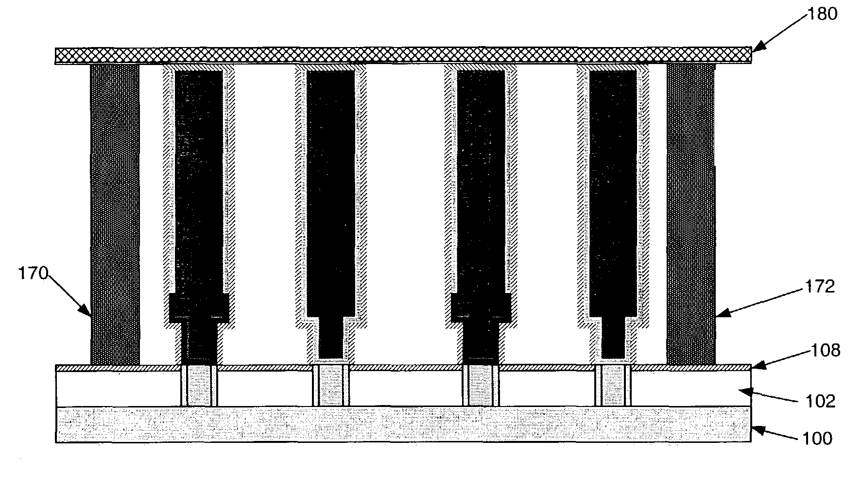
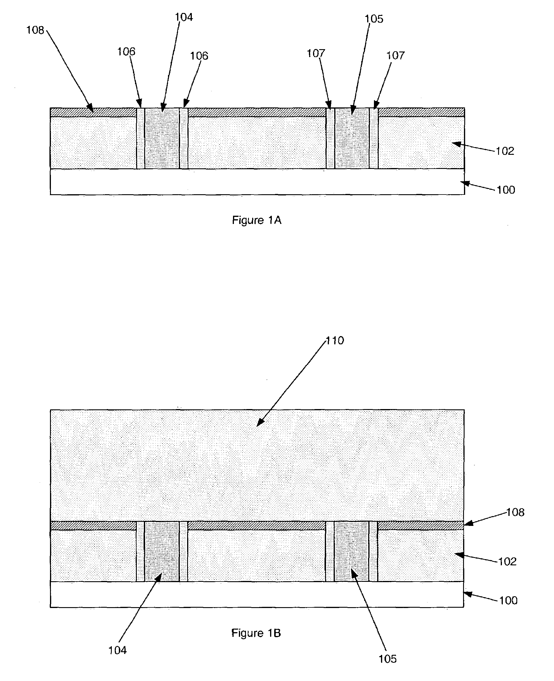
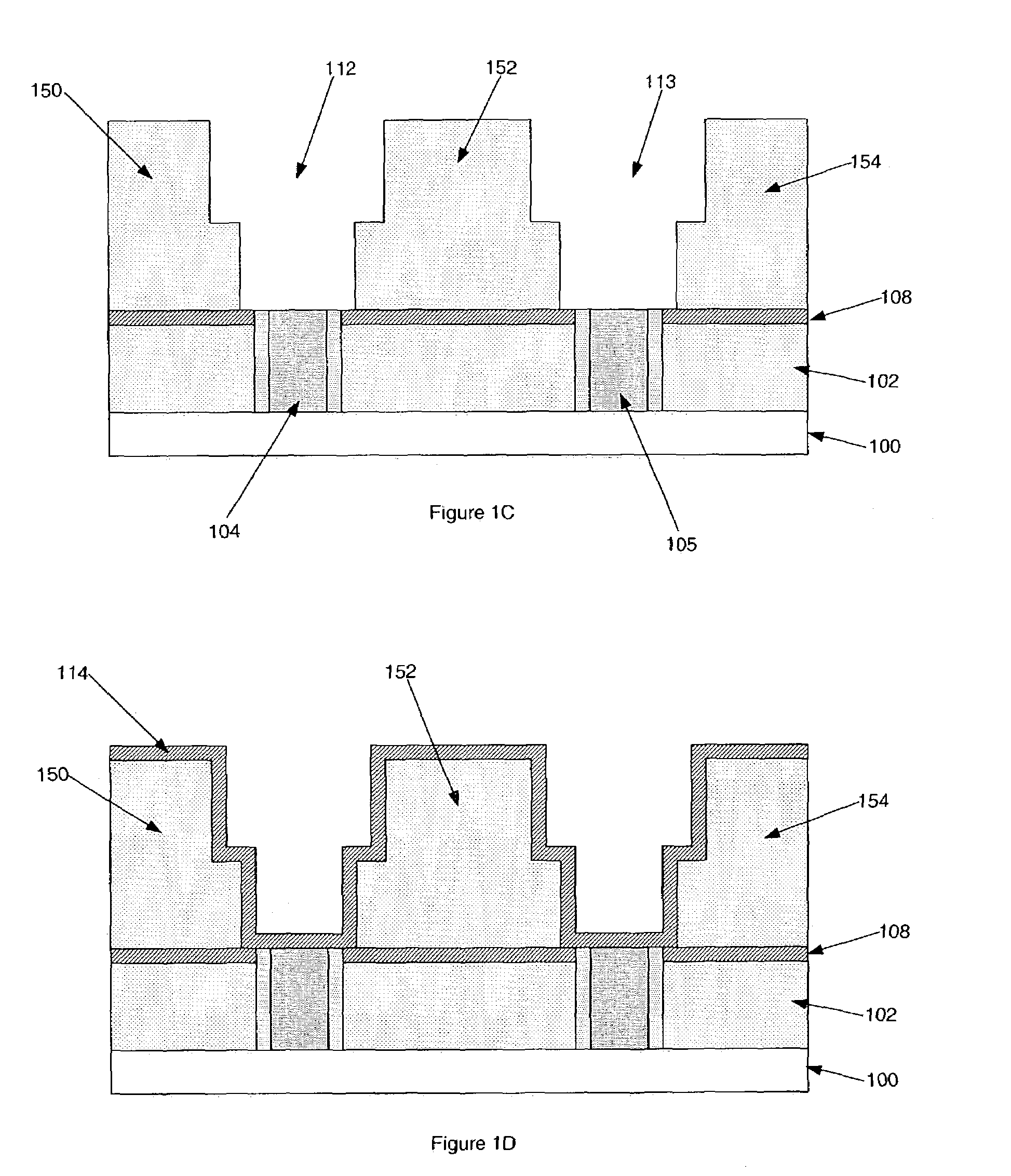
[0007]Referring to FIG. 1A, a microelectronic structure, such as a semiconductor structure, is depicted having a substrate layer (100) adjacent a dielectric layer (102), which is positioned between an etch stop layer (108) and the substrate layer (100). The dielectric layer (102) and etch stop layer (108) are cross sectionally interrupted by via conductive layers (104, 105) crossing the dielectric layer (102) and etch stop layer (108). Each of the via conductive layers (104, 105) is isolated from the dielectric layer ...


PUM


Abstract

Method and structure for integrating conductive and dielectric materials in a microelectronic structure having air gaps are disclosed. Certain embodiments of the invention comprise isolating dielectric layers from conductive layers using an etch stop layer to facilitate controlled removal of portions of the dielectric layers and formation of air gaps or voids. Capping and peripheral structural layers may be incorporated to increase the structural integrity of the integration subsequent to removal of sacrificial material.

Description

BACKGROUND OF THE INVENTION[0001]Low dielectric constant materials are used as interlayer dielectrics in microelectronic devices, such as semiconductor-devices, to reduce the resistance-capacitance (“RC”) delay and improve device performance. As device sizes continue to shrink, the dielectric constant (“k”) of the material between metal lines must also decrease to maintain the improvement. Certain low-k materials have been proposed, including various carbon-containing materials such as organic polymers and carbon-doped oxides. The eventual limit for a dielectric constant is k=1, which is the value for a vacuum. Methods and structures have been proposed to incorporate void spaces or “air gaps” in attempts to obtain dielectric constants closer to k=1. One major issue facing air gap technology is how to remove sacrificial material to facilitate multi-layer structures. Another major issue facing air gap technology is how to facilitate air gap creation while providing a structure which c...

Claims


Application Information

Patent Timeline
Patent Type & Authority Patents(United States)
IPC IPC(8): H01L21/76H01L23/48H01L23/52H01L29/00H01L21/4763H01L21/768H01L23/522H01L23/532
CPCH01L21/76807H01L21/7682H01L23/53295H01L21/76831H01L23/5222H01L21/76829H01L21/76801H01L23/53238H01L2924/0002H01L2924/00
Inventor LIOU, HUEY-CHIANG
Owner TAHOE RES LTD
Why Eureka
Try Eureka