Split waveguide phased array antenna with integrated bias assembly

Active Publication Date: 2006-02-07
ROCKWELL COLLINS INC
View PDF13 Cites 50 Cited by
  • Summary
  • Abstract
  • Description
  • Claims
  • Application Information

AI Technical Summary

Benefits of technology

[0017]It is an advantage of the present invention to provide a convenient mounting method for a phase shifter/TTD device on a circuit board substrate prior to attachment to waveguide half sections.
[0018]It is an advantage of the present invention to simplify interconnection of phase shifter

Problems solved by technology

This is very difficult to accomplish with conventional extruded waveguide technology since the circuit board 22 is somehow slid inside and secured to the waveguide 21.
For large arrays, the assembly of this architecture is costly because many circui

Method used


Image

  • Split waveguide phased array antenna with integrated bias assembly
  • Split waveguide phased array antenna with integrated bias assembly
  • Split waveguide phased array antenna with integrated bias assembly

Examples


Example

[0034]The invention described herein greatly improves and expands on conventional waveguide phased array technology in which planar microwave / millimeter wave circuitry is used to implement phase shifting or true time delay (TTD) circuits.

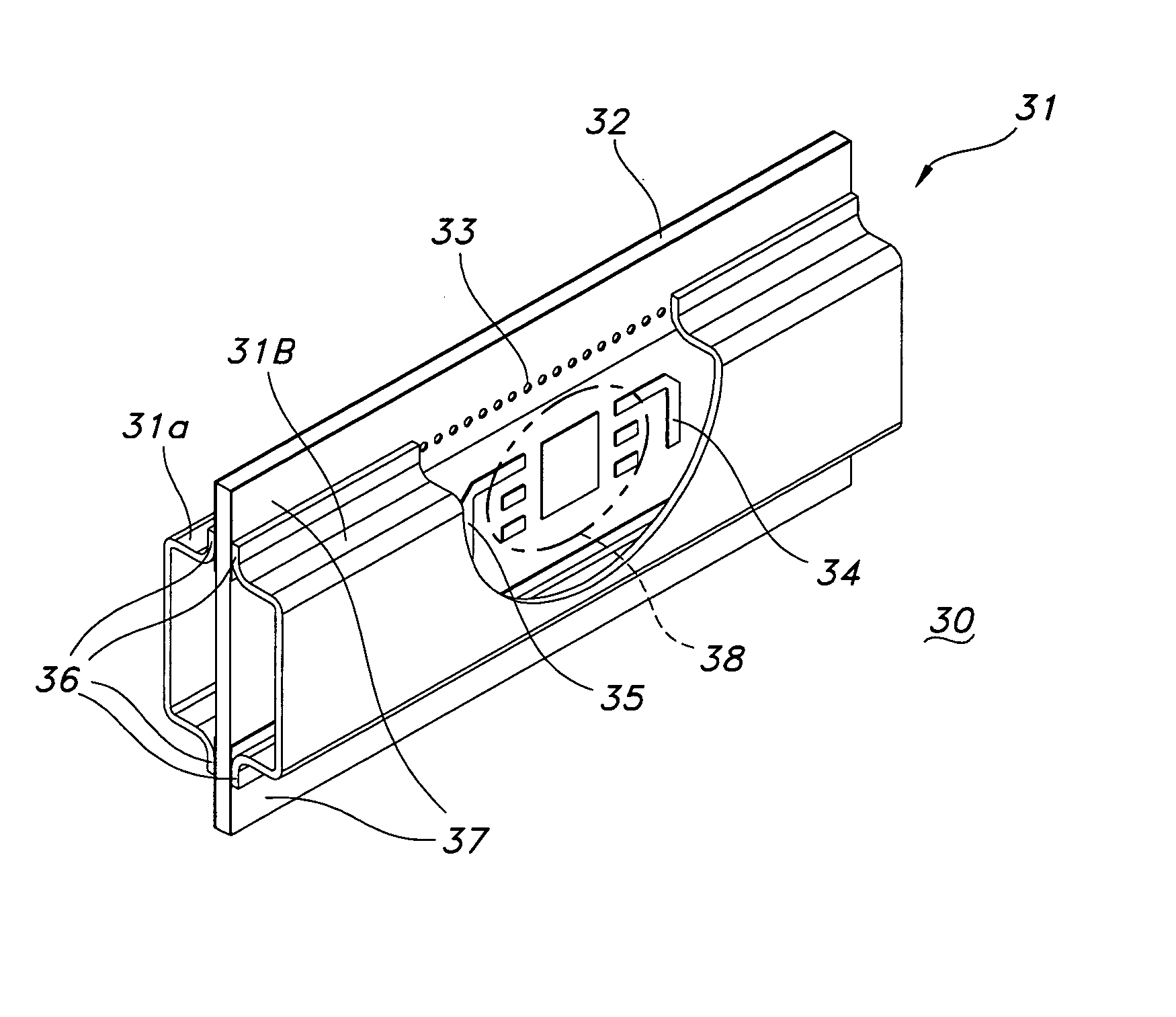
[0035]A split waveguide structure 30 of the present invention incorporating a planar transmission line-to-waveguide transition circuit board substrate 32 is illustrated in FIG. 3. A split waveguide 31 is comprised of two symmetrical waveguide portions, 31a and 31b with each portion having a channel or U-shaped cross section. Other shapes may be used that have at least one plane of symmetry. These two symmetrical waveguide portions 31a and 31b are conductively joined to a RF ground on opposite sides the circuit board substrate 32 at four low electrical resistance joints 36 between the circuit board substrate 32 and the symmetrical waveguide portions 31a and 31b. With this embodiment the RF planar circuit board substrate 32 and metallic split waveguid...


PUM


Abstract

A phased array antenna is made up of linear arrays. Each of the linear arrays has a printed circuit board spine. Split waveguides are formed from two symmetrical portions conductively joined to ground on opposite sides of the printed circuit board spine. Planar transmission line-to-waveguide transitions are mounted on the printed circuit board spine within the split waveguides. Phase shifter/TTD devices are mounted on the circuit board spine within the split waveguides for steering the phased array antenna beam. Bias and control circuitry is etched on the circuit board spine for biasing and controlling the phase shifter/TTD devices. The phased array antenna may be made up of the linear arrays combined into a two-dimensional array and fed with a waveguide feed or a printed feed manifold attached to the printed wiring board spine.

Description

CROSS REFERENCE TO RELATED APPLICATIONS[0001]The present application is related to co-pending application Ser. No. 10 / 273,459 filed on Oct. 18, 2002 entitled “A Method and Structure for Phased Array Antenna Interconnect” invented by John C. Mather, Christina M. Conway, and James B. West and to Ser. No. 10 / 273,872 entitled “A Construction Approach for an EMXT-Based Phased Array Antenna” invented by John C. Mather, Christina M. Conway, James B. West, Gary E. Lehtola, and Joel M. Wichgers. The co-pending applications are incorporated by reference herein in their entirety. All applications are assigned to the assignee of the present application.BACKGROUND OF THE INVENTION[0002]This invention relates to antennas, phased array antennas, and specifically to a phased array antenna utilizing planar phase shifter or true time delay (TTD) devices and a structure for embedded control and bias lines.[0003]Phased array antennas offer significant system enhancements for both military and commercia...

Claims


Application Information

Patent Timeline
IPC IPC(8): H01Q13/00
CPCH01Q13/06H01Q21/061H01Q21/0006
Inventor WEST, JAMES B.MATHER, JOHN C.
Owner ROCKWELL COLLINS INC
Why Eureka
Try Eureka