FC chip system stacked fan-out package structure and preparation method thereof

A packaging structure and chip system technology, which is applied in semiconductor/solid-state device manufacturing, semiconductor/solid-state device components, semiconductor devices, etc., can solve the problems that multiple FC chips cannot be stacked, cannot meet industrial needs, and limit system integration. , to achieve the effects of improving packaging efficiency, simplifying interconnection methods, and simplifying the process

Inactive Publication Date: 2018-01-26
58TH RES INST OF CETC
View PDF4 Cites 6 Cited by
  • Summary
  • Abstract
  • Description
  • Claims
  • Application Information

AI Technical Summary

Problems solved by technology

Due to the development of electronic products towards higher system integration density, the use of single chip packaging technology has gradually been unable to meet the needs of the industry, and multiple FC chips in traditional packaging cannot be stacked, which limits the integration of the system

Method used


Image

  • FC chip system stacked fan-out package structure and preparation method thereof
  • FC chip system stacked fan-out package structure and preparation method thereof
  • FC chip system stacked fan-out package structure and preparation method thereof

Examples


Embodiment Construction

[0031] The present invention will be further described below in conjunction with specific drawings and embodiments.

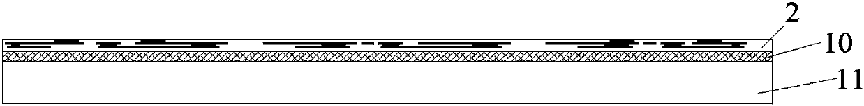
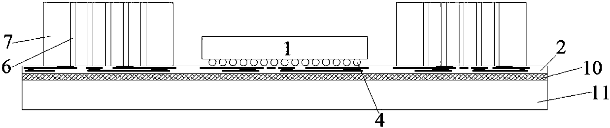
[0032] Such as Figure 7 As shown: in order to effectively realize the stack packaging of FC chips, the present invention includes a stack package formed by two FC chips 1, and the backs of the two FC chips 1 in the stack package are in contact with each other; The rewiring layer 2, the lower rewiring layer 3 is arranged under the stacked package, and the corresponding chip bumps 4 of the two FC chips 1 in the stacked package are respectively electrically connected to the upper rewiring layer 2 and the lower rewiring layer 3;

[0033] A symmetrically distributed vertical interconnection adapter board 7 is arranged on the outside of the stacked package, and the required connection between the upper rewiring layer 2 and the lower rewiring layer 3 is performed through the through-hole connectors 6 in the vertical interconnection adapter board 7 respectively. elec...


PUM


Abstract

The invention relates to a FC chip system stacked fan-out package structure and a preparation method thereof. The package structure comprises a stacked package body formed by two FC chips. The back surfaces of the two FC chips in the stacked package body are abutted against each other. An upper rewiring layer is arranged above the stacked package body; a lower rewiring layer is arranged under thestacked package body; and corresponding chip bumps of the two FC chips in the stacked package body are electrically connected with the upper rewiring layer and the lower rewiring layer. The outer sides of the stacked package body are provided with symmetrically-distributed vertical interconnection transfer boards respectively; and through required electrical connection between through-hole connectors in the vertical interconnection transfer boards and the upper rewiring layer and the lower rewiring layer, required signal interconnection and/or signal leading-out end transfer between the two FCchips in the stacked package body is realized. The package structure is compact in structure, can effectively realize stacked package of the FC chips, can simplify process and improve packaging efficiency, and is safe and reliable.

Description

technical field [0001] The invention relates to a packaging structure and a preparation method thereof, in particular to an FC chip system stacking fan-out packaging structure and a preparation method thereof, belonging to the technical field of integrated circuit packaging. Background technique [0002] With the rapid development of semiconductor integrated circuit technology, the integration level is getting higher and higher, and the number of input and output (I / O) terminals on the chip is increasing rapidly. Wire bonding (WB) technology and tape-loaded automatic bonding (TAB) technology have It cannot meet the development needs of highly integrated semiconductors. Flip-chip (FC) interconnection technology is to arrange I / O terminals in the shape of a grid array on the entire chip surface, and the chip is directly mounted on the wiring board in an upside-down manner. The pads realize electrical connection, more I / O terminals can be arranged in the same area, and the pit...

Claims


Application Information

Patent Timeline
Patent Type & Authority Applications(China)
IPC IPC(8): H01L25/065H01L23/498H01L21/48H01L21/60H01L23/488H01L23/48
CPCH01L2224/16145
Inventor 高娜燕张荣臻明雪飞
Owner 58TH RES INST OF CETC
Why Eureka
Try Eureka