
Multi-ported memory cell

a memory cell and multi-port technology, applied in the field of digital electronic circuits, can solve the problems of essentially no stability for the 4-port memory device, difficult to have both stability and writability for the multi-port cell, etc., and achieve the effect of enhancing the operation margin and improving the beta-ratio

Inactive Publication Date: 2006-02-14
ORACLE INT CORP
View PDF25 Cites 13 Cited by
  • Summary
  • Abstract
  • Description
  • Claims
  • Application Information

AI Technical Summary

Benefits of technology

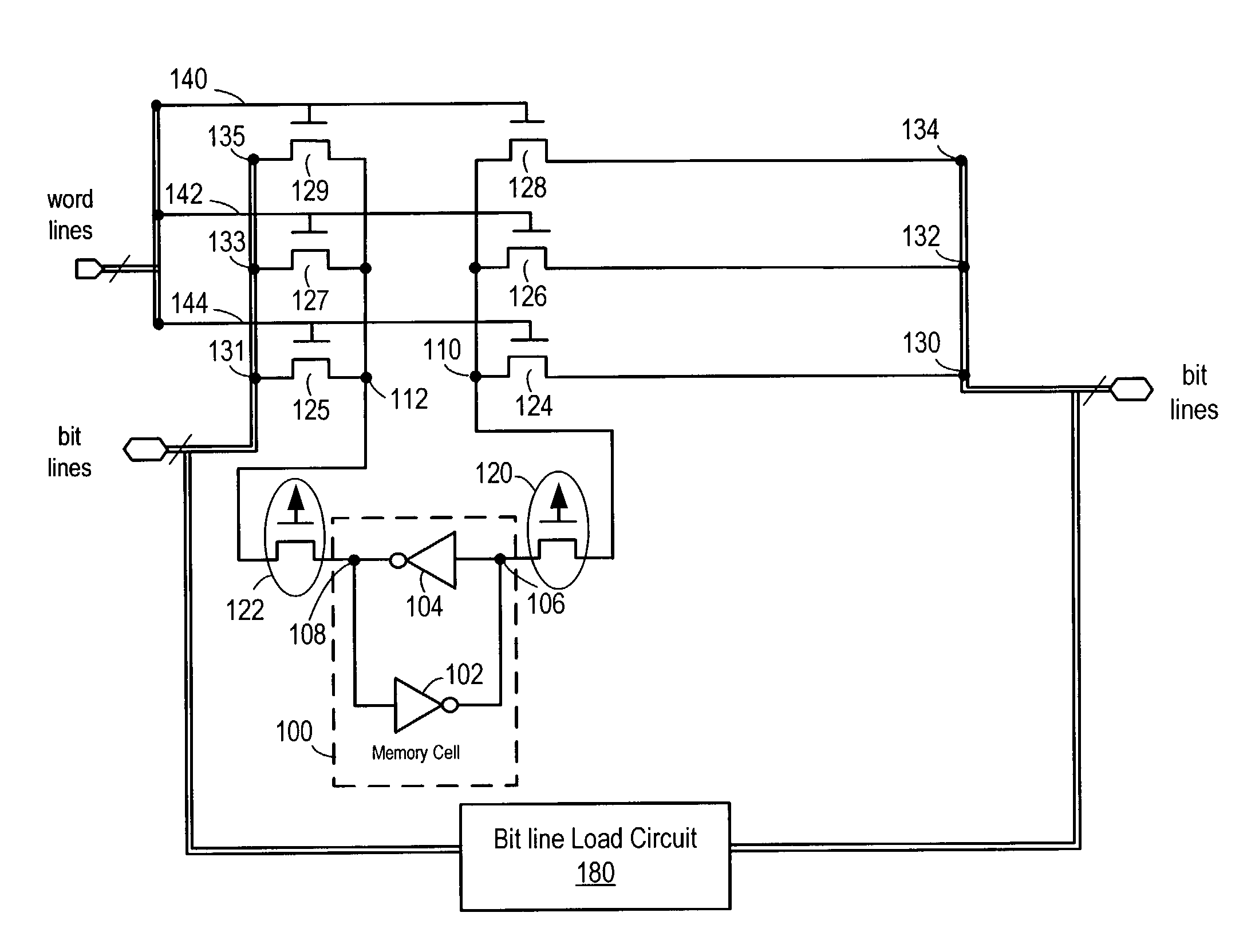
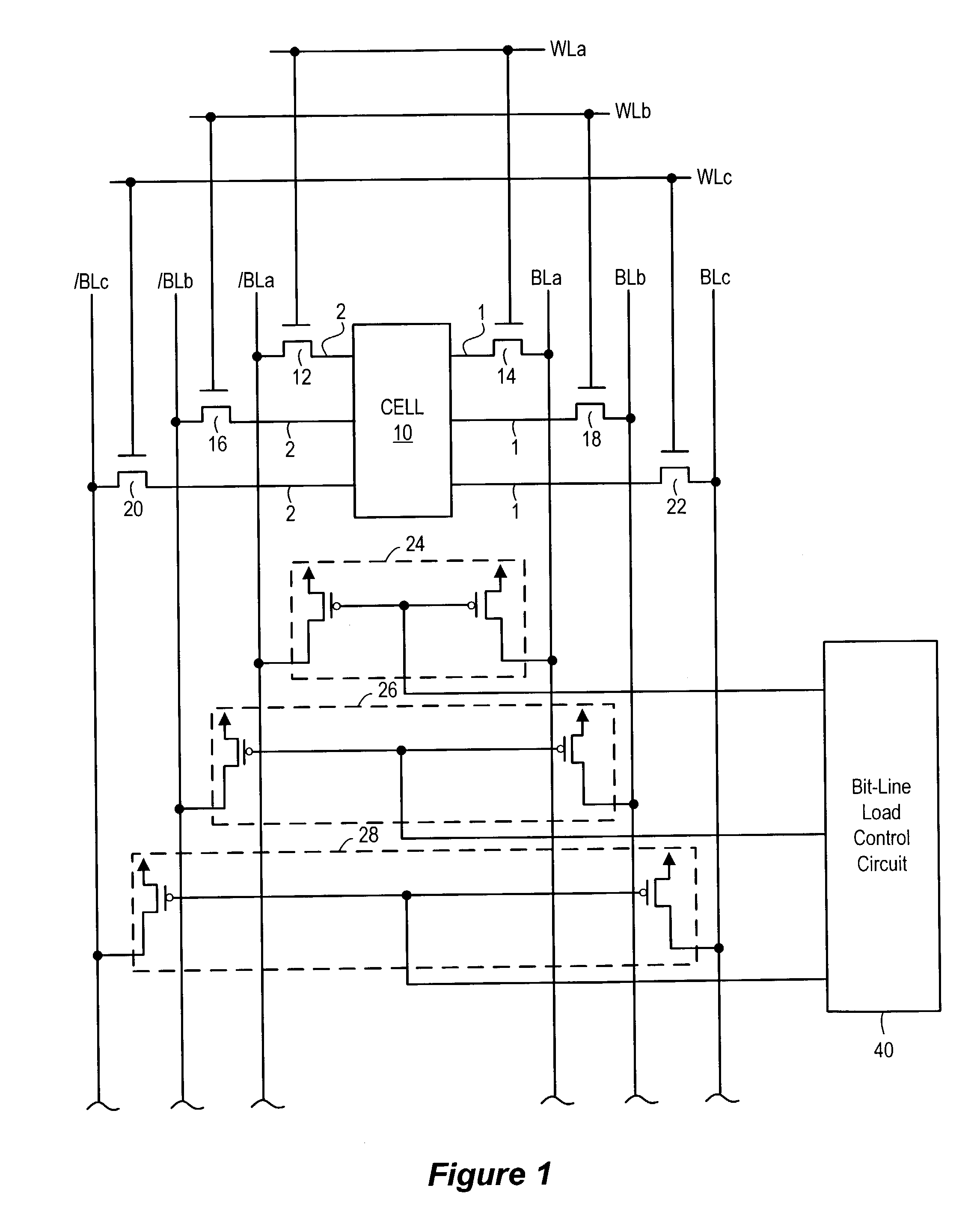
"The present invention provides a semiconductor memory device that includes a plurality of memory cells, each having a first and second memory node. A current limiting device is coupled to each memory node, which acts as a current limiter to improve the beta-ratio and enhance operation margin for both cell stability and writability. Additionally, a multi-port semiconductor memory device is provided that includes a plurality of memory cells, each having a first and second memory node, and a current limiting device is coupled to each memory node. A plurality of transfer devices are coupled to each current limiting device, which has a current path connected between a bit line and the current limiting device to which it is coupled. The technical effects of the present invention include improved stability and writability of the memory cells, as well as faster data transfer between the bit line and the memory cells."

Problems solved by technology

As the port number M increases for a multi-port memory, it becomes increasingly difficult to have both stability and writability for the multi-ported cell when non-writing wordlines are activated.
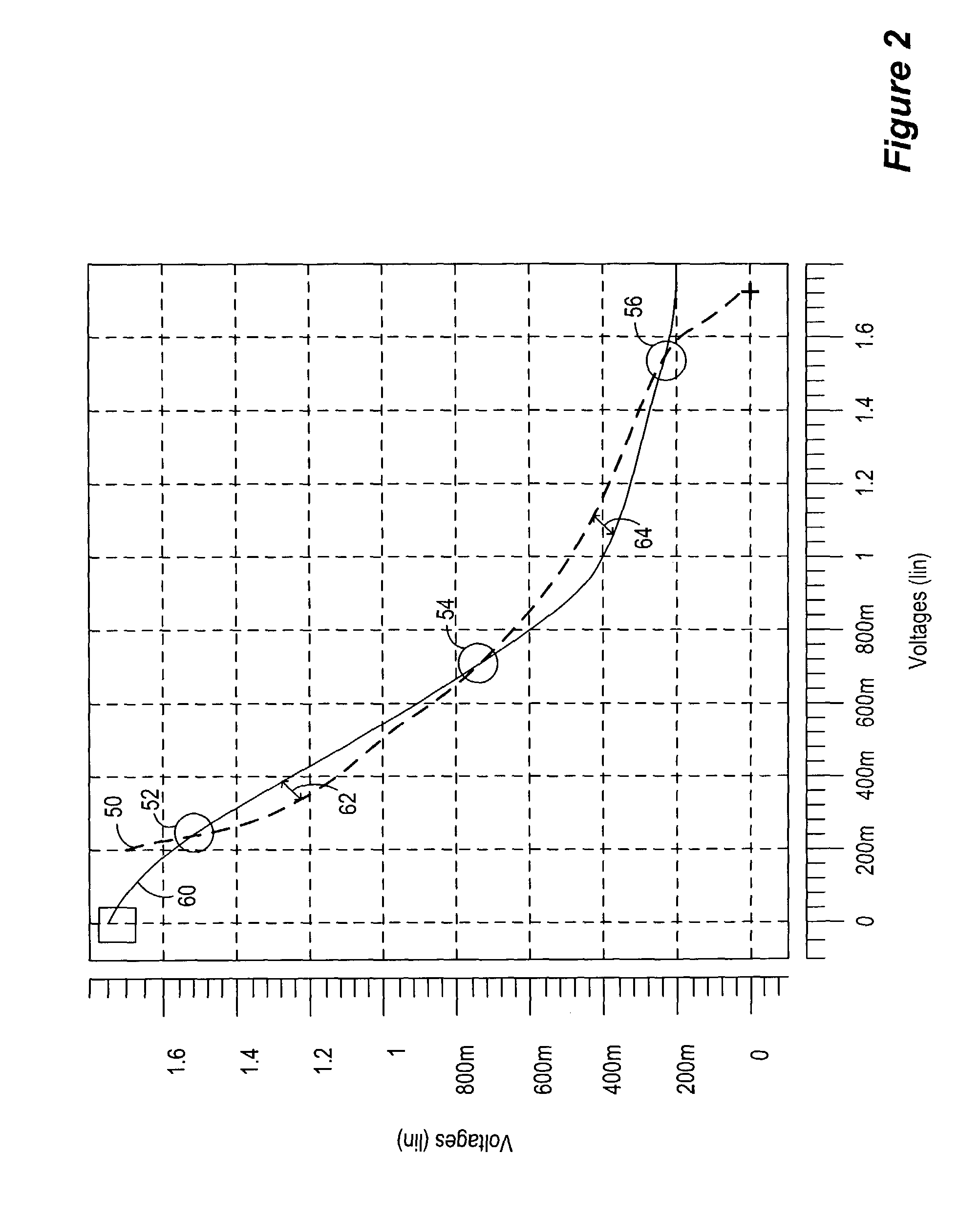
As shown in FIG. 3, there is essentially no stability for the 4-port memory device because there is no spread between the waveforms.

Method used


Image

  • Multi-ported memory cell
  • Multi-ported memory cell
  • Multi-ported memory cell

Examples


Embodiment Construction

[0024]In addition to providing a memory design that is stable (in terms of retaining the data content stored in the memory cell), there is a competing and potentially conflicting need for writability that must be balanced in the memory design. For example, memory stability is promoted by having smaller transfer or access gate sizes and larger NMOS gate sizes in the memory cell inverters. The ratio of these sizes is referred to as the beta-ratio, which is bigger for more stable memory designs, meaning that the NMOS driver gate in the memory cell inverters is larger and the transfer gate is smaller. However, with multi-port memories, the effective increase in the transfer gate size (because of the additional transfer gates for the additional ports) reduces the beta-ratio, meaning that the cell stability is diminished. Thus, to obtain stable memory cell operation, there is minimum beta-ratio value required for memory cell stability.

[0025]At the same time, cell writability is improved w...


PUM


Abstract

A multi-port semiconductor memory device is provided with current limiting transistor devices interposed between the memory cell and the bit line transfer gates for multiple bit line pairs. Where each bit line pair represents a memory port that is connected to the memory cell during read and write operations, the current limiting transistor devices effectively reduce the current flow from non-writing bit lines, thereby improving memory writability. In addition, the current limiting transistor devices effectively reduce the current flow to non-reading bit lines, thereby improving memory stability.

Description

BACKGROUND OF THE INVENTION[0001]1. Field of the Invention[0002]The present invention generally relates to the field of digital electronic circuits, specifically, semiconductor memory devices adapted for use with computer systems. In one aspect, the present invention relates to a semiconductor memory device which has a multi-port function.[0003]2. Description of the Related Art[0004]Generally, a multi-port memory is a memory device having a number of ports for reading and writing and corresponding address and control ports, such that multiple locations in the memory can be simultaneously accessed. A plurality of word lines and a plurality of bit lines are connected to each memory cell of the multi-port memory. Multi-port memories may be used in a variety of applications, such as a cache memory which functions as a memory common to the CPUs incorporated in a multi-CPU system, or as an image memory in which the same address must be accessed at the same time.[0005]With multi-port memor...

Claims


Application Information

Patent Timeline
Patent Type & Authority Patents(United States)
IPC IPC(8): G11C8/00G11C11/00G11C7/12
CPCG11C7/12
Inventor TAKAYANAGI, TOSHINARI
Owner ORACLE INT CORP
Learn More