Electronic component

a technology of electronic components and lead wires, applied in the direction of electrical apparatus casings/cabinets/drawers, coupling device connections, semiconductor/solid-state device details, etc., can solve the problems of low workability of lead wires connecting to the circuit board, bad electrical contact, low contact strength of wires, etc., and achieve high reliability

Active Publication Date: 2006-02-21
JVC KENWOOD CORP A CORP OF JAPAN
View PDF10 Cites 12 Cited by
  • Summary
  • Abstract
  • Description
  • Claims
  • Application Information

AI Technical Summary

Benefits of technology

[0008]A purpose of the present invention is to provide a highly reliable electronic component with an adequate amount of resin.

Problems solved by technology

The known electronic component, however, has low workability in connecting the lead wires to the circuit board.
However, in known electronic components, such as, the one disclosed in Japanese Un-examined Patent publication No. 5 (1993)-55432, when external force is applied, in a direction of pulling, to the lead wires pulled out from the casing to connect the circuit board and an external device, stress is focused on contact points of the circuit board and the clipleads, and also the clip leads and the lead wires, thus causing bad electrical contact.
Especially, the contact points of the dip leads and the lead wires have low contact strength, and hence often suffer from bad electrical contact.

Method used


Image

  • Electronic component
  • Electronic component
  • Electronic component

Examples


first embodiment

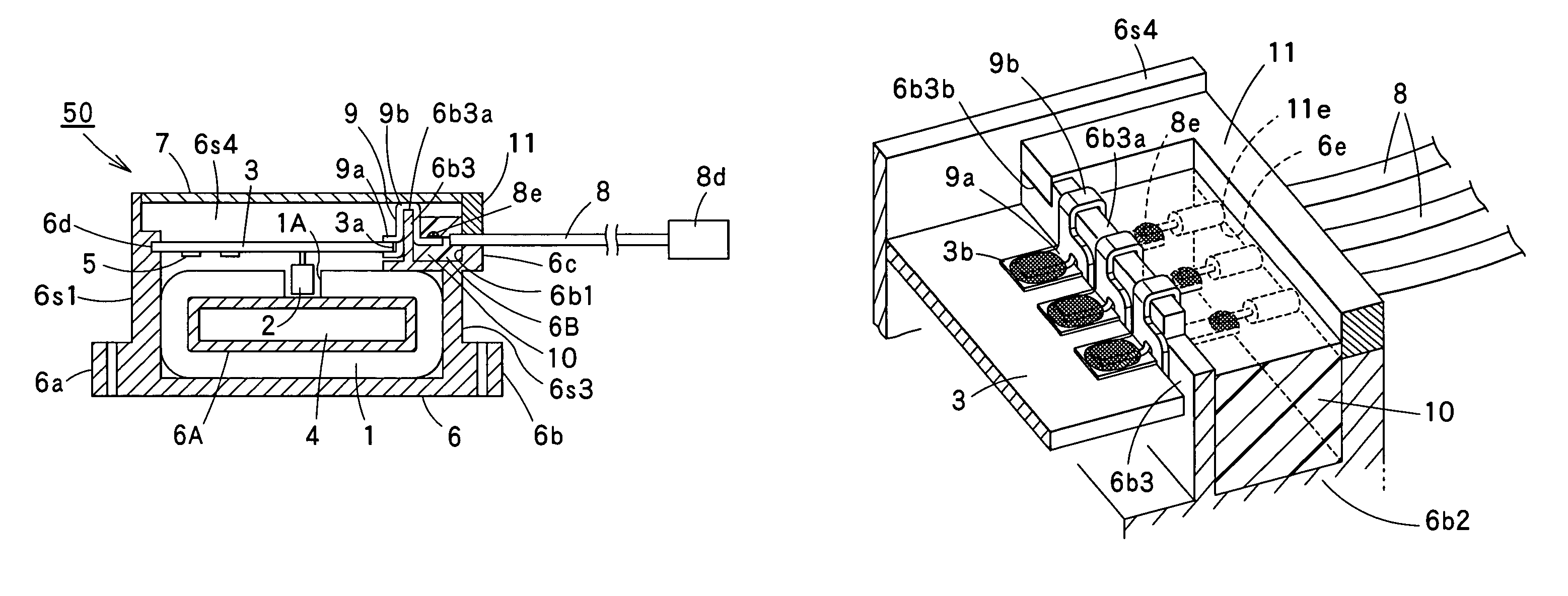
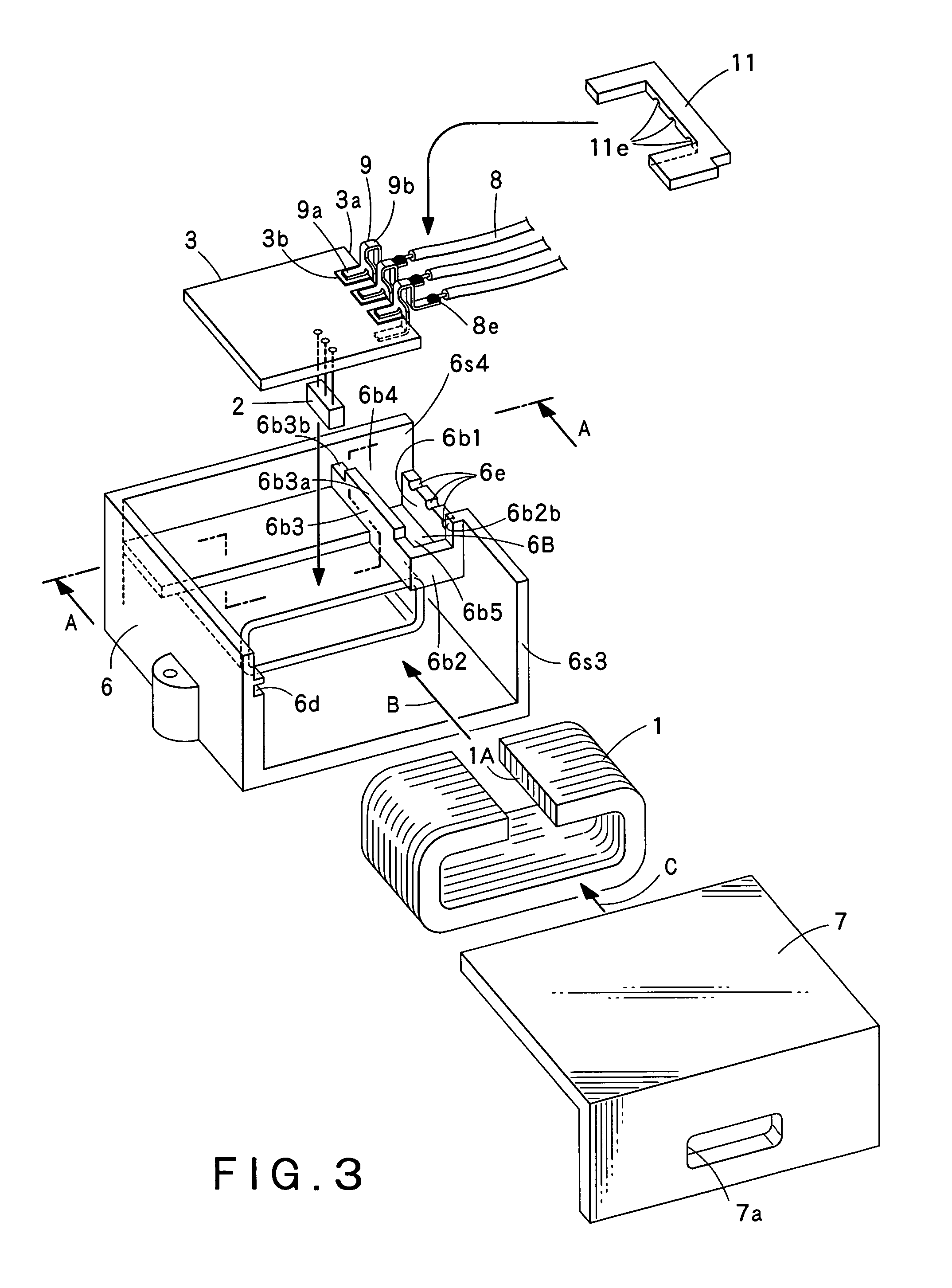
[0028]FIGS. 2A, 2B, 3 and 4 show a current sensor 50, an electronic component according to the present invention. FIG. 2A show a cross section of the first embodiment. FIG. 2B is a perspective view of the first embodiment. FIG. 3 is an assembly view illustrating how to assemble the first embodiment. FIG. 4 is a partially enlarged view of the first embodiment. FIG. 2A is a view taken on line A—A of FIG. 3. Epoxy resin 10 is indicated with dots for its cross section only in FIG. 2A so that elements covered with resin 10 can been seen.

[0029]The current sensor 50 (the first embodiment) accurately detects a large current flowing through a current path with no loads applied thereto.

[0030]As shown in FIG. 2A, a hall element 2 mounted on a circuit board 3 is situated in a magnetic gap 1A of a loop-like magnetic core 1. A conducting wire (not shown) is inserted into the magnetic core 1. A current flowing through the conducting wire is detected by the hall element 2.

[0031]The magnetic core 1 ...


PUM


Abstract

An electronic component has a casing having a resin injecting section having at least one wall. At least one circuit board is housed in the casing, next to the resin injecting section via the wall. At least one lead terminal is provided in the casing. The lead terminal has a first end and a second end, and a middle section connected between the first and second ends. The first end of the lead terminal is connected to the circuit board in a way that the middle section of the lead terminal is provided as straddling the wall of the resin injecting section. Also provided is at least one lead wire having a third end and a fourth end. The third end of the lead wire is connected to the second end of the lead terminal in the resin injecting section. The fourth end of the lead wire is pulled out from the casing. The third end of the lead wire and the second end of the lead terminal connected to each other are embedded in resin injected in the resin injecting section whereas the middle section of the lead terminal straddling the wall of the resin injecting section is not embedded in the resin. Instead of straddling the wall of the resin injecting section, the middle section of the lead terminal may be inserted into an opening provided on the wall and connected to the circuit board.

Description

BACKGROUND OF THE INVENTION[0001]The present invention relates to an electronic component having a circuit board housed in a casing, and input and output lead wires. Particularly, the present invention relates to an electronic component having a circuit board housed in a casing, and input and output lead wires fixed to the casing with resin injected in the casing.[0002]An electronic component having a circuit board housed in a casing, and input and output lead wires for electrical connections is disclosed in Japanese Un-examined Utility Model No. 7 (1995)-36071.[0003]This known electronic component is a current sensor for detecting a current flowing through an electric wire. Lead wires soldered to the circuit board are pulled out from the casing and connected to an external device, etc.[0004]The known electronic component, however, has low workability in connecting the lead wires to the circuit board. Because, it is required to wind the lead wires around terminals fixed to the circu...

Claims


Application Information

Patent Timeline
Patent Type & Authority Patents(United States)
IPC IPC(8): H05K7/02H01L23/08H01R13/405H01R13/52H01R43/24H05K3/34H05K5/00
CPCH01R13/5216H05K3/3405H05K5/0091H01R13/405H01R43/24H05K2201/10977H05K2201/10287H05K2201/10386H05K2201/10962
Inventor TAKABATAKE, NARITOMONAKAMURA, HIROSHI
Owner JVC KENWOOD CORP A CORP OF JAPAN
Why Eureka
Try Eureka