Isolation chamber arrangement for serial processing of semiconductor wafers for the electronic industry

a technology of serial processing and semiconductor wafers, applied in the direction of furniture, instruments, charge manipulation, etc., can solve the problems of difficult to maintain or achieve uniformity and consistency of products in these processes, large clean rooms, and high operating costs, so as to simplify loading and unloading, the indexing mechanism is simplified, and the treatment time is minimized

Inactive Publication Date: 2006-03-07
SEMLGEAR INC
View PDF2 Cites 253 Cited by
  • Summary
  • Abstract
  • Description
  • Claims
  • Application Information

AI Technical Summary

Benefits of technology

[0021]The support housing beneath the outer lower housing may include a bellows to permit the longitudinal advancement and withdrawal of the support column of the housing while maintaining the ambient relationship within the isolation chamber. A treatment plate and isolation housing lift and retraction mechanism is also arranged within the support housing to provide the vertical advance and vertical withdrawal of the treatment plate from a semiconductor wafer supported on the wafer support pins on the wafer ring. A vacuum and / or sensors may extend through one or more of the support housings to provide suction to a wafer on the plate for holding purposes. Sensors may provide temperature information about the wafer and or the wafer thereon. Indexed rotational movement of the rotatable index plate advances subsequent semiconductor wafers to each respective treatment module for sequential treatment as that index plate is rotated about its central axis. The robotic loading and unloading of semiconductor wafers occurs from a radially outwardly disposed location with respect to the process table. This peripherally disposed wafer manipulation, instead of from a center of table location, permits simpler indexing mechanism and greatly simplifies the loading and unloading of the semiconductor wafers at that particular loading and unloading module location in the sequence at the process table.
[0022]The treatment plate has a radially directed channel spaced at least partially thereacross. The depth of the channel in the treatment plate is greater than the depth of the grooves for accommodating the wafer support pins thereon. This permits the robotic loading and unloading arm to move or remove a wafer onto the radially newly directed support pins and then subsequently downwardly therefrom to permit the support of that wafer on those support pins without disturbing that semiconductor wafer and without engaging the treatment plate.
[0023]Thus what has been shown is an apparatus for the serial processing of semiconductor wafers from an initial loading of an indexable rotatable plate through a circumferential arrangement of locations at separate treatment modules thus through an unloading operation of that semiconductor wafer after its treatment process. Each independent treatment module effects an isolation chamber processing to permit ambient conditions to be effected upon that semiconductor wafer at that particular location in the process table. By this stepped indexing and complete isolation as each individual wafer is individually processed, treatment times may be minimized and treatment effectiveness may be maximized and equipment costs may be reduced due to the simplicity of the operational features of the present apparatus.

Problems solved by technology

Such a system, however, requires large clean rooms, and they operate under expensive operating conditions.
Uniformity and consistency of a product is difficult to maintain or achieve in these processes.
Such prior art operations in either a belt or batch process are also often very expensive and very complicated.

Method used


Image

  • Isolation chamber arrangement for serial processing of semiconductor wafers for the electronic industry
  • Isolation chamber arrangement for serial processing of semiconductor wafers for the electronic industry
  • Isolation chamber arrangement for serial processing of semiconductor wafers for the electronic industry

Examples


Embodiment Construction

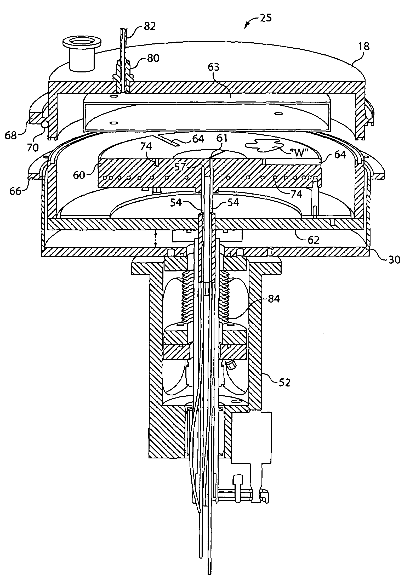
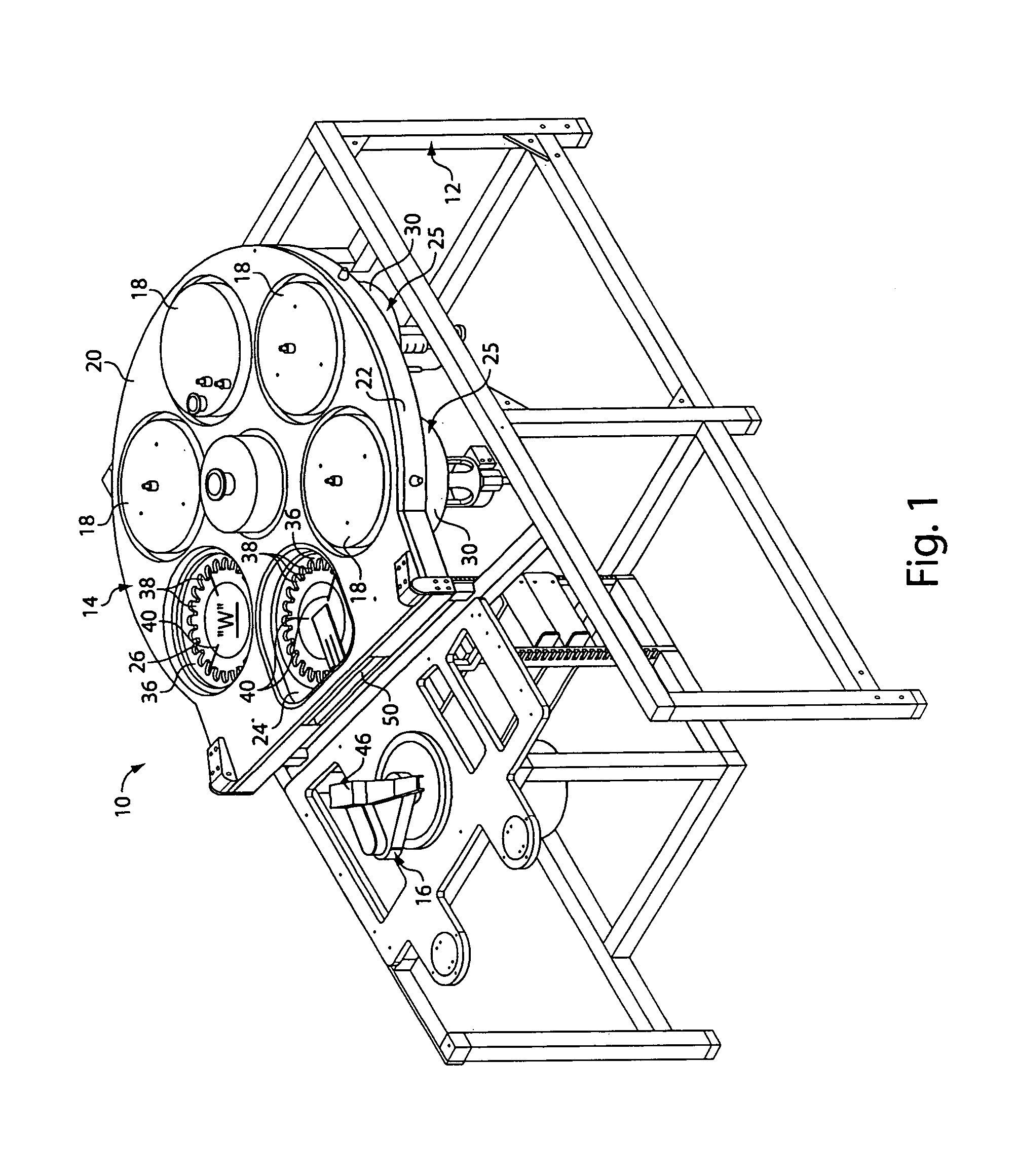
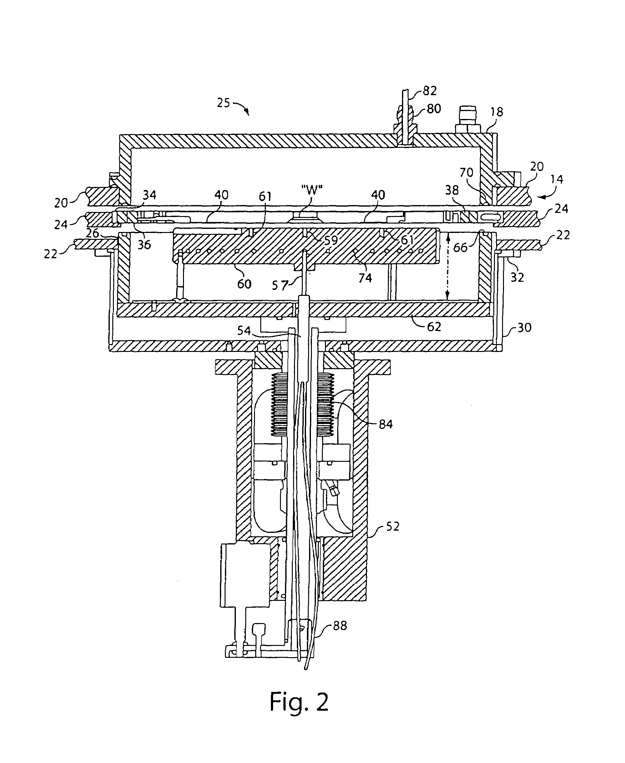
[0036]Referring now to the drawings in detail, and particularly to FIG. 1, there is shown the present invention which comprises a wafer processing arrangement 10 for the sequential isolated treatment processing of semiconductor wafers. The processing arrangement 10 comprises a frame support 12 for a wafer process table 14 and a wafer feed and removal robot arrangement 16 thereadjacent. The wafer process table 14 comprises a plurality of housing covers 18 each positioned on a stationary upper plate 20 as part of a treatment module for each position in the process of treatment of the semiconductor wafers. The housing cover 18 may be changable to permit changing of treatment of the wafers “W” as they go through the process described herein below.

[0037]The wafer process table 14 also includes a stationary lower housing platen 22 which surrounds a central transmission unit (not shown for clarity) which rotatively indexes a rotary index plate 24 between a plurality of treatment modules 25...


PUM

PropertyMeasurementUnit
semiconductoraaaaaaaaaa
sizeaaaaaaaaaa
suctionaaaaaaaaaa

Abstract

An apparatus for the treatment of semiconductor wafers, comprising a supportive frame and a process table arranged on the supportive frame. The process table comprises a stationary upper platen and a stationary lower plate. An intermediate indexing plate is rotatively arranged between the upper platen and the lower plate. At least one wafer support pin is attached to the indexing plate for the support of a wafer by the indexing plate. An upper housing is arranged on the upper platen and an outer lower housing is arranged on the lower plate. A displacable lower isolation chamber is disposed within the outer lower housing, being displacable against the indexing plate to define a treatment module between the upper housing and the lower isolation chamber in which the wafer is treated. A wafer supporting treatment plate is arranged within the lower isolation chamber, for controlled rapid treatment of a wafer within the treatment module.

Description

[0001]This is a divisional application of U.S. patent application Ser. No. 10 / 186,823, filed Jul. 1, 2002 now U.S. Pat. No. 6,827,789, which is incorporated herein by reference.BACKGROUND OF THE INVENTION[0002]1. Field of the Invention[0003]This invention relates to apparatus and methods for the treatment and processing of semiconductor wafers.[0004]2. Prior Art[0005]Semiconductor wafers are utilized in the modern electronics industry for the production of very large scale integrated (VLSI) circuits and Ultra Large Scale Integrated (UlSI) circuits and chips and the like. Such semiconductor wafers must go through a wide variety of high manufacturing standards steps in order to produce a perfect semiconductor product.[0006]During that production process, the wafers must be treated by a series of sequential steps. The processing of these wafers may include oxidation, ion implantation, thermal annealing, deposition, etching, passivation and packaging. The thermal annealing and solder re...

Claims


Application Information

Patent Timeline
Patent Type & Authority Patents(United States)
IPC IPC(8): H01L21/30B65G49/07C23C16/00C23F1/00H01L21/00H01L21/306H01L21/66H01L21/677H01L21/687
CPCH01L21/6719H01L21/67748H01L21/68785Y10S414/139Y10S414/135
Inventor LEE, CHUNGHSINZHANG, JIANSIMONELLI, DARREN MMULLINS, KEITH D.WASSEN, DAVID A.
Owner SEMLGEAR INC
Why Eureka
Try Eureka