Well structure in high voltage device

Inactive Publication Date: 2006-03-07
INTELLECTUAL DISCOVERY CO LTD
View PDF3 Cites 1 Cited by
  • Summary
  • Abstract
  • Description
  • Claims
  • Application Information

AI Technical Summary

Benefits of technology

[0008]A well structure in a high voltage device is disclosed which is capable of improving performance and reliability of the device and realizing higher-integration of the device, by improving a well breakdown voltage and preventing charge-up and latch-up at a substrate.

Problems solved by technology

As such, in case of the NAND flash memory, there occurs a problem where the high voltage device is formed by making the distance between the N-well 12 and the P-well 13 20 μm or greater.
As described above, the conventional well structure in the high voltage device has limitations in higher-integration of the flash memory or the semiconductor device that requires the high well breakdown voltage.

Method used


Image

  • Well structure in high voltage device
  • Well structure in high voltage device
  • Well structure in high voltage device

Examples


Embodiment Construction

[0021]The disclosed well structure will now be described in detail in connection with preferred embodiments with reference to the accompanying drawings.

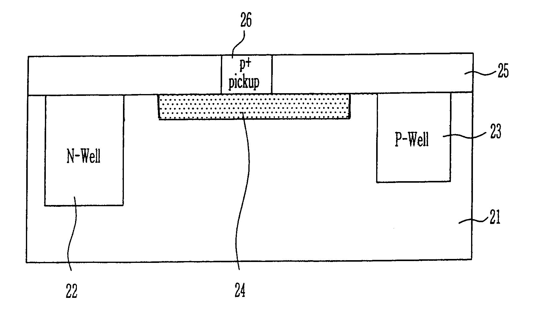
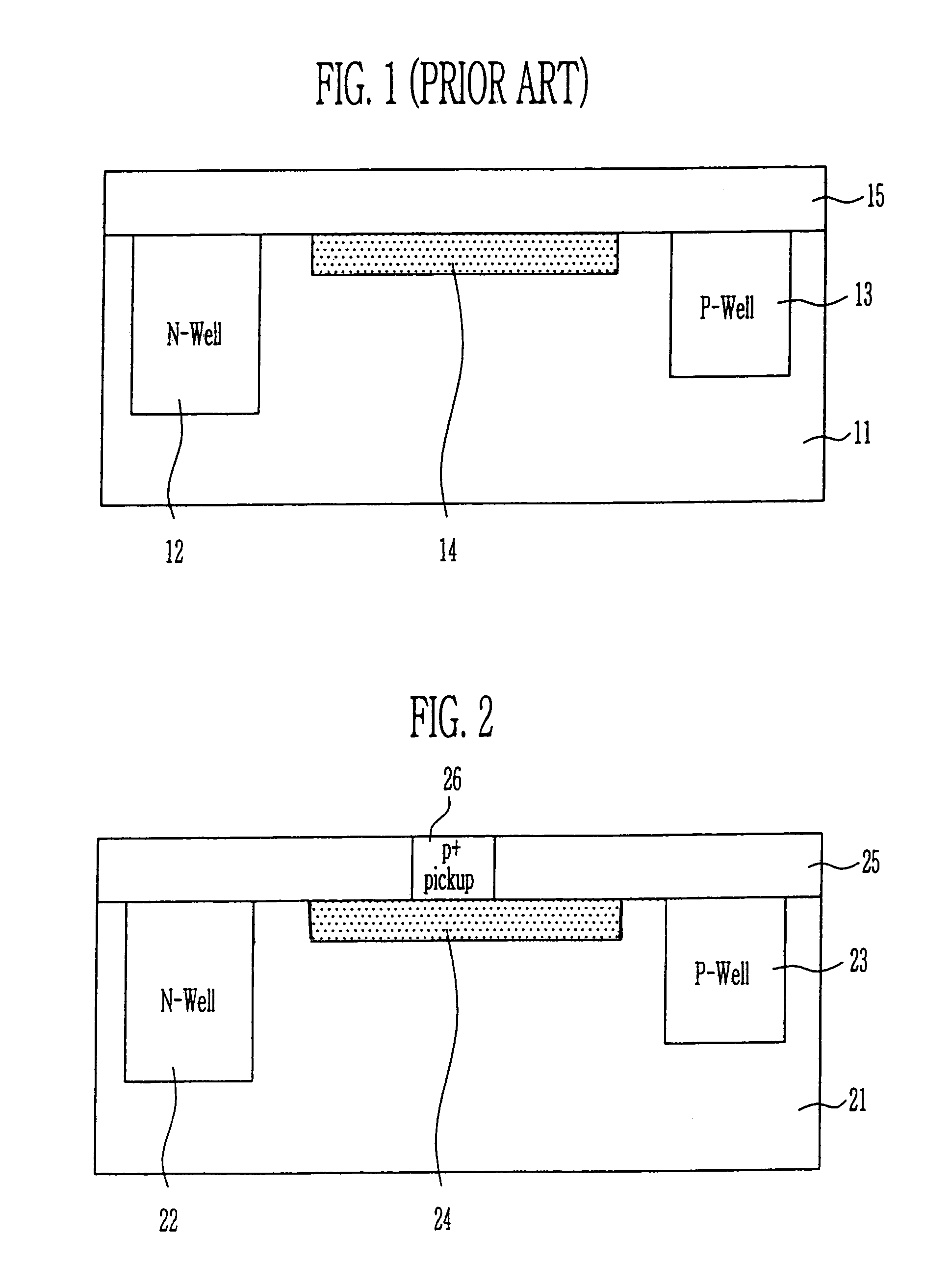
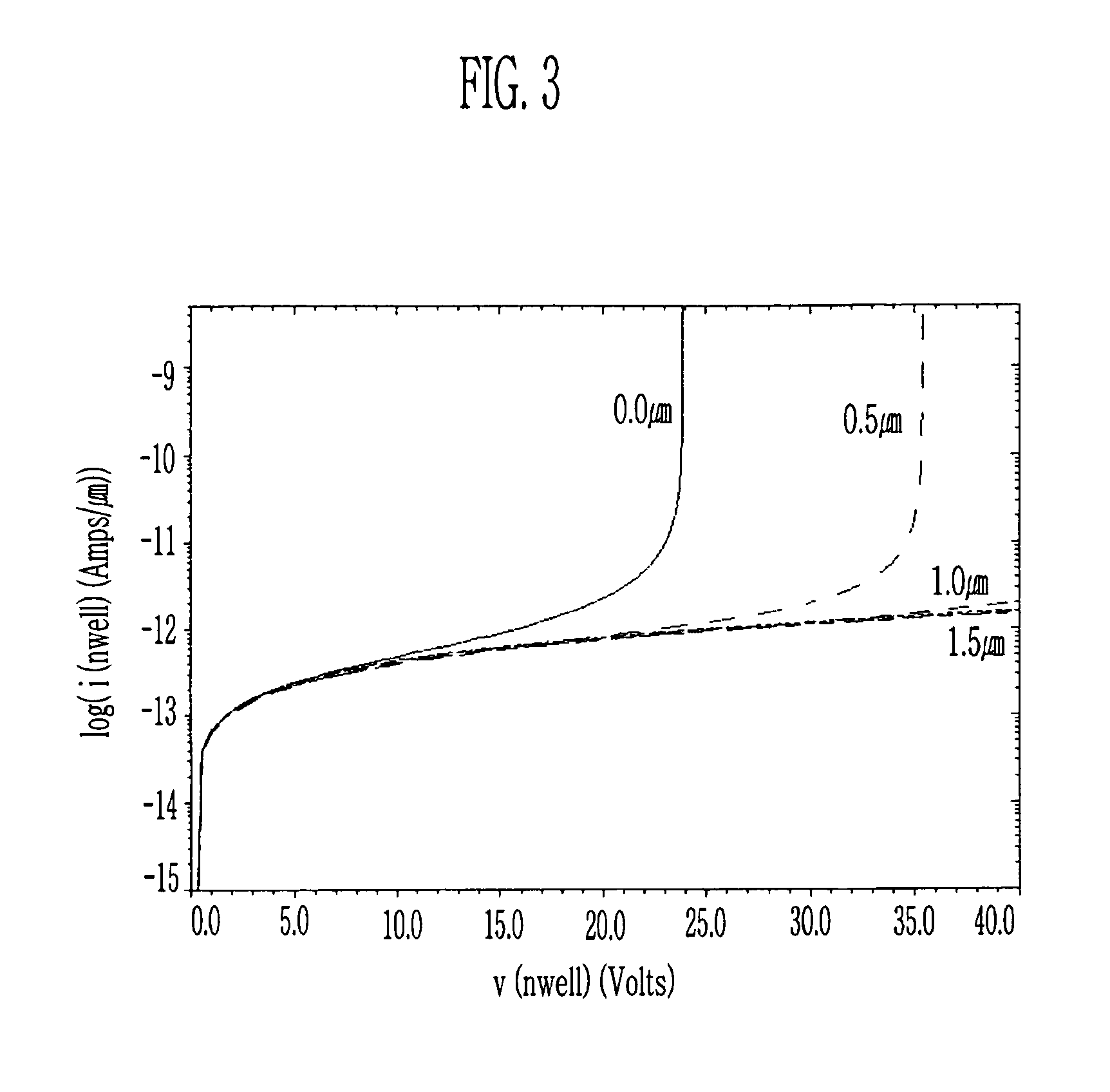
[0022]FIG. 2 is a cross-sectional view illustrating a well structure in a disclosed high voltage device. The proposed well structure may be applied to a NAND type flash memory, an NOR type flash memory and all the semiconductor devices, which require a high voltage.

[0023]Referring to FIG. 2, a first well 22 is formed by implanting an impurity of a conductive type different than the substrate 21 into the substrate 21. A first transistor for a high voltage is contained in the first well 22 by means of a common process. A second well 23 is isolated from the first well 22 and is formed by implanting an impurity of the same conductive type as the substrate 21 into the substrate 21. A second transistor for a high voltage is contained in the second well 23 by means of a common process. A field stop implant region 24 is formed between the fi...


PUM


Abstract

A well structure in a high voltage device comprises a first well formed in a substrate, the first well having an opposite conductive type from the substrate; a second well isolated from the first well, the second well having the same conductive type as the substrate; a field stop implant region formed between the first well and the second well and spaced apart from each of the first well and the second well by a given distance, the field stop implant region having the same conductive type as the substrate; and a pick-up region overlapped on the field stop implant region, the pick-up region having the same conductive type as the field stop implant region.

Description

BACKGROUND[0001]1. Technical Field[0002]A well structure in a high voltage device is disclosed which is capable of improving a well breakdown voltage (BVDSS) and preventing charge-up and latch-up at a substrate in the high voltage device used in a flash memory.[0003]2. Discussion of the Related Art[0004]In general, the flash memory is mainly classified into an NOR type and a NAND type depending on a shape in which memory cells are connected to bit lines. A high voltage is used in the NAND type flash memory or the NOR type flash memory in order to perform a program operation or an erase operation. In order for the NAND type flash memory to perform the program operation or the erase operation, a voltage of about 20V is required. Further, in order for the NOR type flash memory to perform the program operation or the erase operation, a voltage of about 14V is needed. In order to apply such high voltage to a cell region, a high voltage device is located in a peripheral circuit region.[00...

Claims


Application Information

Patent Timeline
IPC IPC(8): H01L29/76H01L29/94H01L21/8238H01L21/8247H01L27/092H01L27/115H01L29/06H01L29/78
CPCH01L29/0619H01L29/0615H01L27/115H10B69/00H01L29/78
Inventor PARK, SUNG KEE
Owner INTELLECTUAL DISCOVERY CO LTD
Why Eureka
Try Eureka