
System and method for sensing data stored in a resistive memory element using one bit of a digital count

a resistive memory element and data sensing technology, applied in digital storage, electric analogue stores, instruments, etc., can solve the problems of physical largeness, reduced device reliability, and relatively slow existing mass storage devices

Inactive Publication Date: 2006-03-07
OVONYX MEMORY TECH LLC
View PDF38 Cites 82 Cited by
  • Summary
  • Abstract
  • Description
  • Claims
  • Application Information

AI Technical Summary

Problems solved by technology

A memory characteristic that often times determines whether a given type of memory is suitable for a given application is the volatile nature of the storage.
Both DRAM and SRAM are volatile forms of data storage, which means the memories require power to retain the stored data.
Such mass storage devices are, however, physically large and contain numerous moving parts, which reduces the reliability of the devices.
Moreover, existing mass storage devices are relatively slow, which slows the operation of the computer system or other electronic device containing the mass storage device.
While FLASH provides nonvolatile storage, FLASH is too slow for use as system memory and the use of FLASH for mass storage is impractical, due in part to the duration for which the FLASH can reliably store data as well as limits on the number of times data can be written to and read from FLASH.
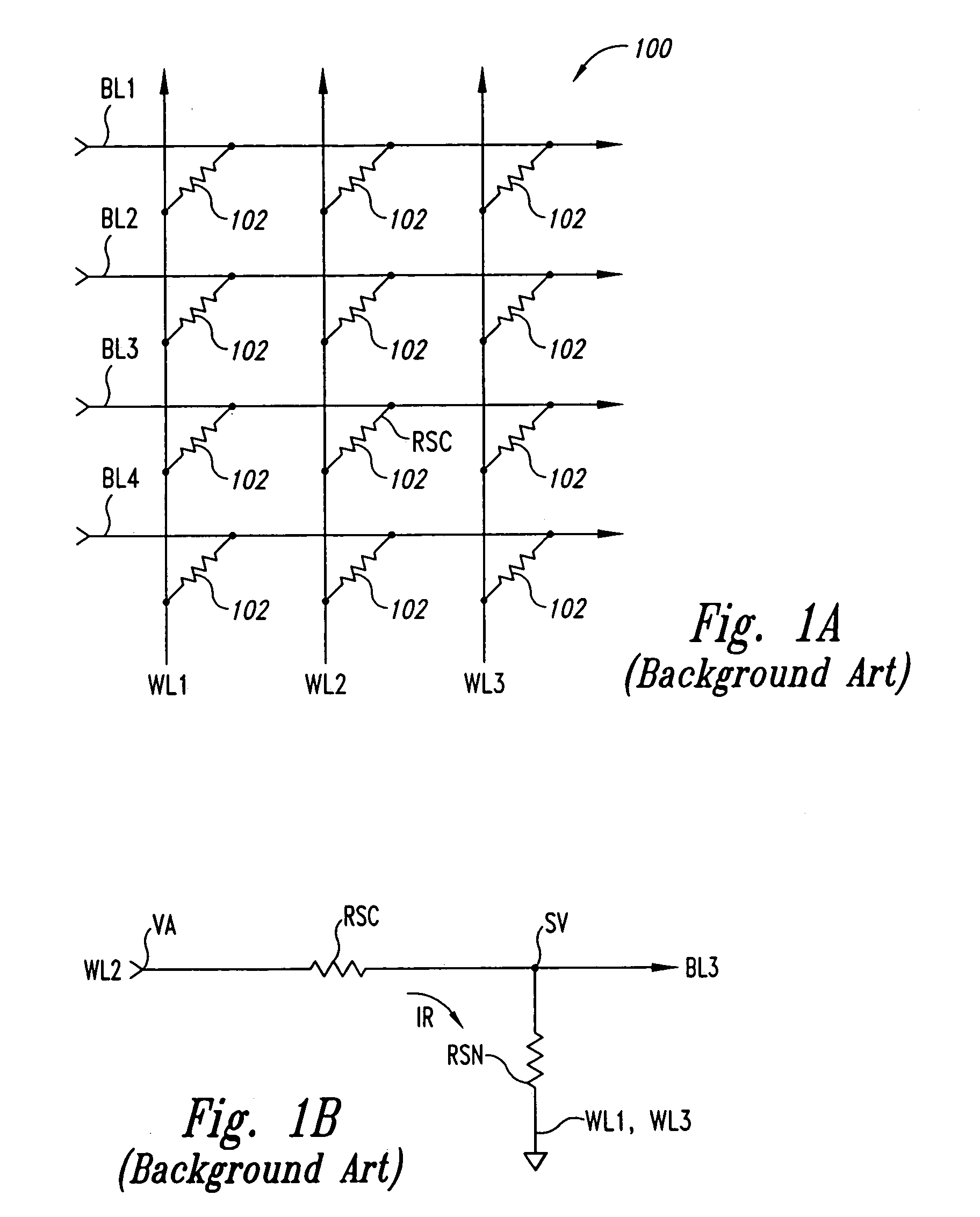
In practice, however, reliable sensing is difficult due, in part, to the relatively small change in the resistance of the memory cell 102 between logic states.
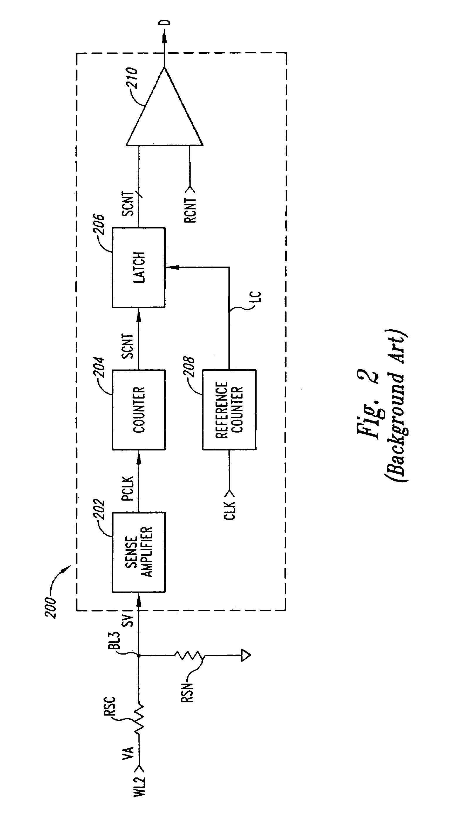
As a result, the RCNT may ideally need to be varied depending on which cell 102 is being selected, which further complicates the circuitry of the read circuit 200.

Method used


Image

  • System and method for sensing data stored in a resistive memory element using one bit of a digital count
  • System and method for sensing data stored in a resistive memory element using one bit of a digital count
  • System and method for sensing data stored in a resistive memory element using one bit of a digital count

Examples


Embodiment Construction

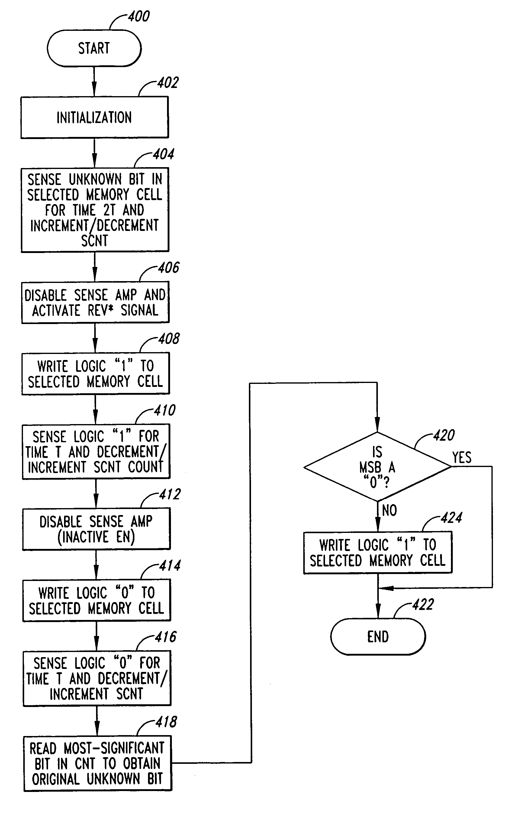
[0024]FIG. 3 is a functional block diagram illustrating a read circuit 300 that generates a sense count SCNT having a most significant bit (MSB) corresponding to the logic state of the data stored in a selected memory cell 102 in the MRAM array 100 of FIG. 1 according to one embodiment of the present invention. In contrast to the prior data circuit 200 of FIG. 2, which generates an N-bit count SCNT that must then be compared to another N-bit reference count RCNT to determine the logic state of the data stored in a selected memory cell 102, the read circuit 300 generates single N-bit count SCNT having a single MSB bit indicating the logic state of data stored in the selected memory cell, as will be explained in more detail below. By eliminating the need to utilize the reference count RCNT and the need to compare two N-bit counts, the data circuit 300 provides a simplified and reliable circuit for reading data from MRAM memory cells. In the following description, certain details are s...


PUM


Abstract

A method and system sense the logic state of an unknown initial data bit stored in a selected resistive memory cell. According to one method, a first count representing the logic state of the unknown initial data bit stored in the selected memory cell is generated. A second count is then generated, and represents a data bit having a first known logic state stored in the selected memory cell. A third count is then generated, and represents a data bit having a second known logic state stored in the selected memory cell. The logic state of the initial unknown data bit stored in the selected memory cell is then determined from the first, second, and third counts.

Description

CROSS-REFERENCE TO RELATED APPLICATION[0001]This application is a divisional of U.S. patent application Ser. No. 10 / 192,463, filed Jul. 9, 2002 now U.S. Pat. No. 6,813,208.TECHNICAL FIELD[0002]The present invention relates generally to integrated circuits, and more specifically to sensing data stored in an integrated circuit memory device.BACKGROUND OF THE INVENTION[0003]Computer systems, video games, electronic appliances, digital cameras, and myriad other electronic devices include memory for storing data related to the use and operation of the device. A variety of different memory types are utilized in these devices, such as read only memory (ROM), dynamic random access memory (DRAM), static random access memory (SRAM), flash memory (FLASH), and mass storage such as hard disks and CD-ROM or CD-RW drives. Each memory type has characteristics that better suit that type to particular applications. For example, DRAM is slower than SRAM but is nonetheless utilized as system memory in ...

Claims


Application Information

Patent Timeline
Patent Type & Authority Patents(United States)
IPC IPC(8): G11C7/02G11C7/06G11C7/20G11C11/16
CPCG11C7/06G11C11/16G11C7/20
Inventor BAKER, R. JACOB
Owner OVONYX MEMORY TECH LLC
Learn More