

Semiconductor memory device
a memory device and semiconductor technology, applied in semiconductor devices, digital storage, instruments, etc., can solve the problem of many holes remaining in the body
- Summary
- Abstract
- Description
- Claims
- Application Information
AI Technical Summary
Benefits of technology
Problems solved by technology
Method used
Image

Examples
first embodiment
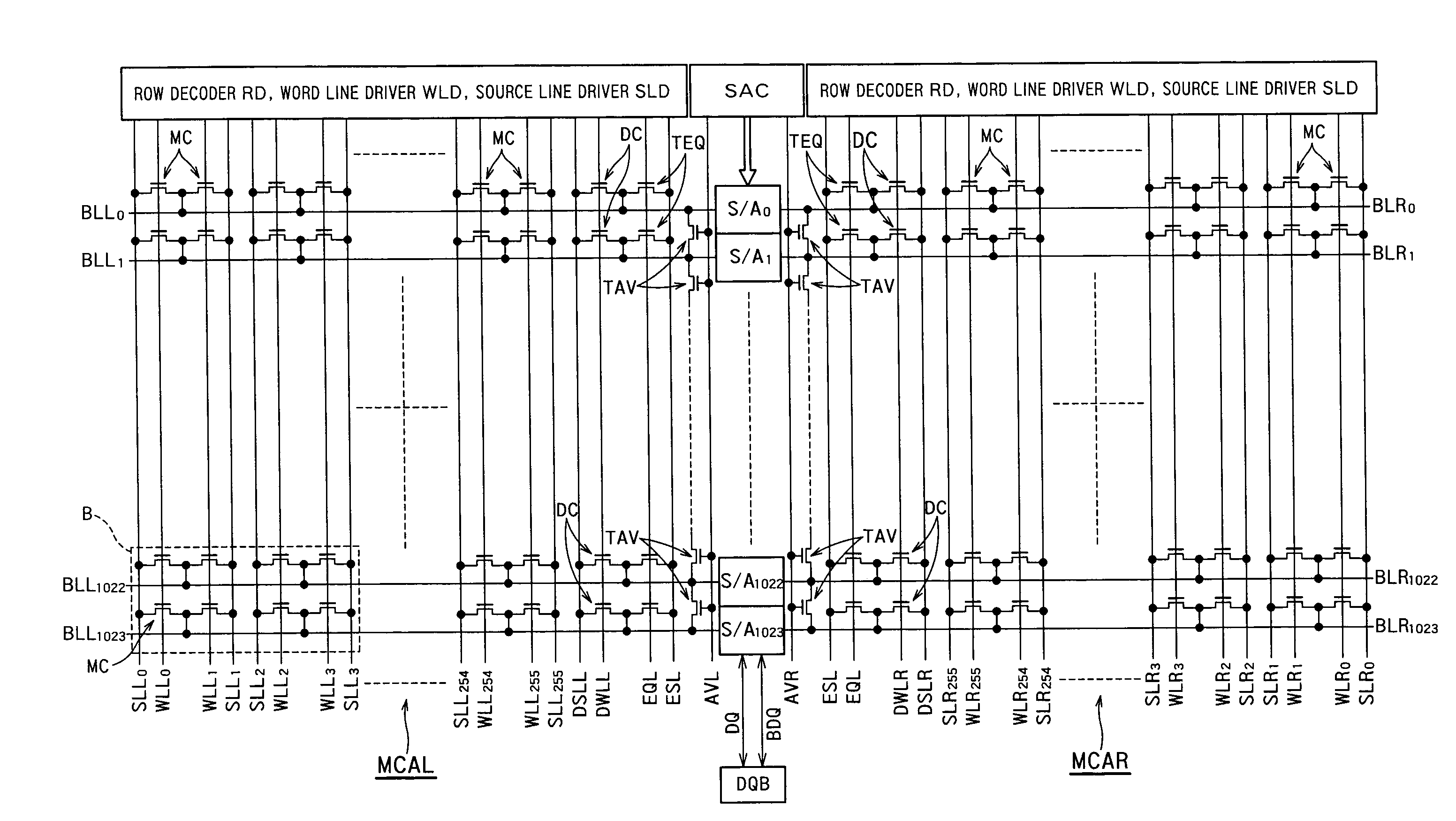
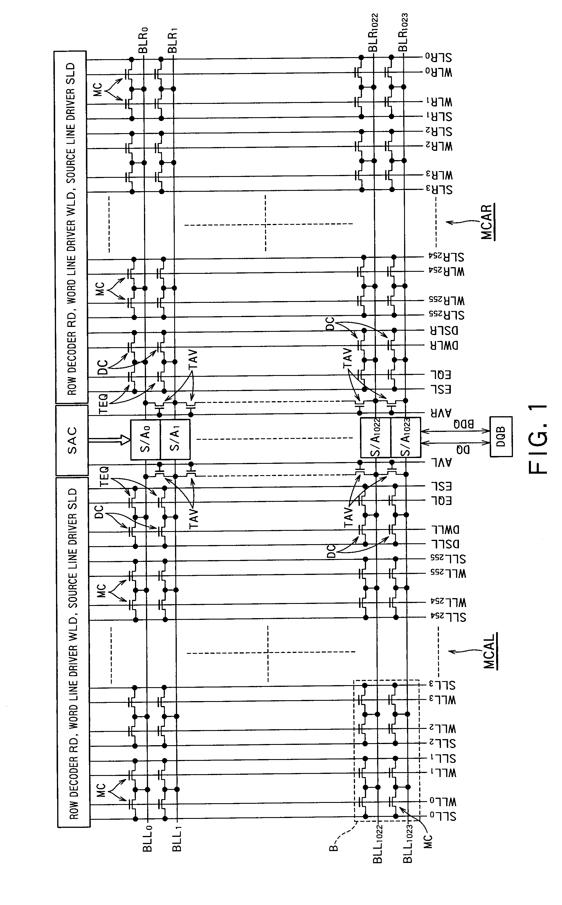
[0051]FIG. 1 shows a configuration of an FBC memory device according to a first embodiment of the present invention. An FBC memory device 100 includes memory cells MCs, dummy cells DCs, word lines WLLi and WLRi (where i is an integer) (hereinafter, also “WLs”), dummy word lines DWLLs and DWLRs (hereinafter, also “DWLs”), bit lines BLLi and BLRi (hereinafter, also “BLs”), sense amplifiers S / Ai (hereinafter, also “S / As”), equalizing lines EQLs, equalizing transistors TEQs, averaging lines AVL and AVR (hereinafter, also “AVs”), source lines SLLi and SLRi (hereinafter, also “SLs”), row decoders RDs, word line drivers WLDs, and source line drivers SLDs.
[0052]The memory cells MCs are arranged two-dimensionally in a matrix and constitute memory cell arrays MCAL and MCAR (hereinafter, also “MCAs”). The word lines WLs extend in a row direction that is a first direction and are connected to gates of the memory cells MCs. 256 word lines WLs are arranged on each of the left and right of the sen...
second embodiment
[0109]FIG. 18 shows a configuration of an FBC memory device according to a second embodiment of the present invention. The FBC memory device shown in FIG. 18 has a so-called 2 cell / bit configuration. Namely, two adjacent bit lines BLL and BBLL, which serve as one bit line pair (hereinafter, “paired bit lines”), are connected to one sense amplifier S / A. Paired bit lines BLR and BBLR corresponding to the paired bit lines BLL and BBLL are connected to the same sense amplifier S / A. The paired bit lines BLL and BBLL and the paired bit lines BLR and BBLR are connected to a pair of cells which store therein one-bit data, respectively. Using one of the paired bit lines BLL and BBLL as a reference, each sense amplifier S / A detects the data stored in the pair of cells. Alternatively, using one of the paired bit lines BLR and BBLR as a reference, each sense amplifier S / A detects the data stored in the cell connected to the other bit line. Therefore, the paired bit lines BLL and BBLL transmit d...
third embodiment
Modification of Third Embodiment
[0135]In the third embodiment, the unselected word line WLL3 sharing the source line SLL2, 3 with the selected word line WLL2 is kept equal in potential (i.e., data holding potential) to the other unselected word lines WLL0, WLL1, and WLL4 to WLL255. If the potential of the unselected word lines WLLs is set to VWLM higher than VWLL, the memory cells MCs connected to the unselected word line WLL3 are often disturbed. In a modification of the third embodiment, the potential of the unselected word line WLL3 sharing the source line SLL2, 3 with the selected word line WLL2 is set lower than that of the other unselected word lines WLLs. Due to this, an FBC memory device according to the modification of the third embodiment includes a driving circuit for word drive lines WDRV0 to WDRV3 different from the conventional techniques.
[0136]The memory cell array in this modification is similar in configuration to those shown in FIG. 23.
[0137]FIG. 30 is a circuit di...
PUM
 Abstract
Description
Claims
Application Information