[0023]Further, according to a seventh aspect of the present invention, a new
system for
interfacing electronic circuits that is created by making a new solder-less breadboard device according to the fifth aspect of the present invention (as shown in FIG. 11) and a new
printed circuit board device according to the sixth aspect of the present invention (as shown in FIG. 12), that are size for size and connection for connection, identical to each other, such that any
electronic circuit that is built on the new solder-less breadboard device can be reproduced exactly on the new
printed circuit board device, thus creating a finished working prototype without having to design and build a unique
printed circuit board for the
electronic circuit.
[0024]Further, according to an eighth aspect of the present invention, a new
system for
interfacing electronic circuits that is created by making a plurality of new solder-less breadboard device according to the seventh aspect of the present invention (as shown in FIGS. 14, 16, 18 and 20) and a plurality of new printed circuit board device according to the seventh aspect of the present invention (as shown in FIGS. 15, 17, 19 and 21) in matching pairs (as shown in FIGS. 14 & 15, 16&17, 18&19, 20&21) such that each pair of devices fit directly into standard sized enclosures, with both devices in each pair having mounting holes that align with the mounting standoffs that exist in the standard sized enclosures, thus allowing mounting without need of modification to either the device or the
enclosure.
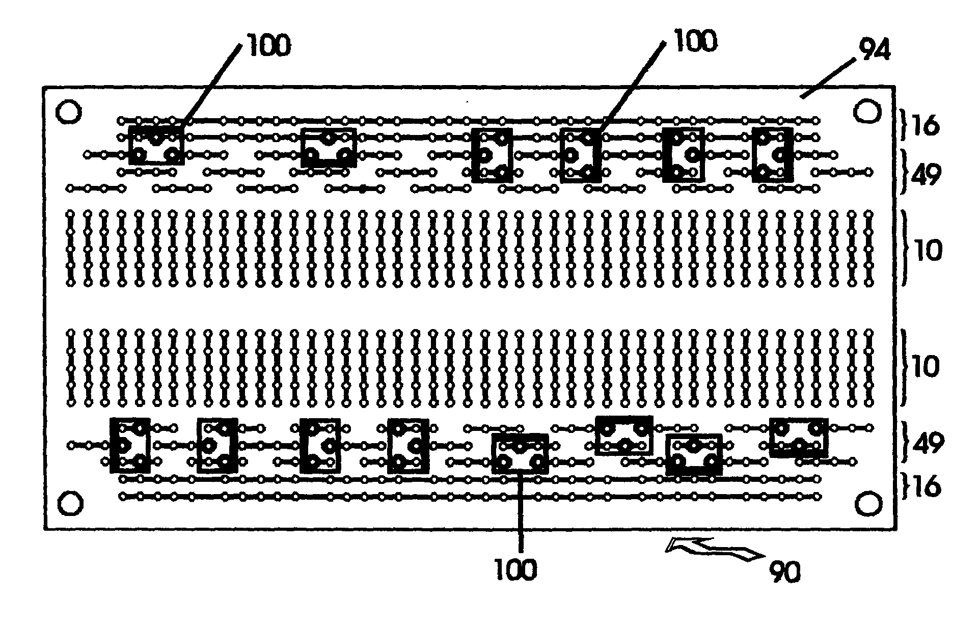
[0025]Further, according to a ninth aspect of the present invention, a new method of interfacing electronic circuits (as shown in FIG. 13) is created by using a new electrical socket device according to the first aspect of the present invention (as shown in FIG. 11) for interconnecting resisters, capacitors, diodes, etc. and connecting transistors, FETs, SCRs, TRIACs, etc. on a solder-less breadboard in an area outside of the terminal strip, such that all interface functions like input
signal conditioning, timing, clocking, inter-circuit level changing and output drivers can exist on the same breadboard without sacrificing
integrated circuit capacity in the terminal strip, thus making breadboarding quicker, easier and neater while building circuits that are cleaner, easier to follow and more compact.
[0026]Further, according to a tenth aspect of the present invention, a new method of interfacing electronic circuits (as shown in FIG. 13) is created by using a new printed circuit board device according to the second aspect of the present invention (as shown in FIG. 12) for interconnecting resisters, capacitors, diodes, etc. and connecting transistors, FETs, SCRs, TRIACs, etc. on a printed circuit prototyping board in an area outside of the terminal strip, such that all interface functions like input
signal conditioning, timing, clocking, inter-circuit level changing and output drivers can exist on the same prototype board without sacrificing
integrated circuit capacity in the terminal strip, thus making prototyping quicker, easier and neater while building circuits that are cleaner, easier to follow and more compact.
[0027]Further, according to an eleventh aspect of the present invention, a new method of interfacing electronic circuits (as shown in FIG. 13) is created by using the new method according to the ninth aspect of the present invention, on a new solder-less breadboard device according to the seventh aspect of the present invention (as shown in FIG. 11) and then exactly reproducing the
electronic circuit by using the new method according to the tenth aspect of the present invention, on a new printed circuit board device according to the seventh aspect of the present invention (as shown in FIG. 12) thus dramatically shortening the time required to go from concept to finished working prototype.
[0028]Further, according to a twelfth aspect of the present invention, a new method of interfacing an electronic circuits (as shown in FIG. 13) is created by using the new method according to the ninth aspect of the present invention, on a new solder-less breadboard device according to the eighth aspect of the present invention (as shown in FIGS. 14, 16, 18 and 20) and then exactly reproducing the electronic circuit by using the new method according to the tenth aspect of the present invention, on a new printed circuit board device according to the eighth aspect of the present invention (as shown in FIGS. 15, 17, 19 and 21) thus dramatically shortening the time required to go from concept to finished working prototype and allowing the new breadboard device or the new printed circuit board device to fit directly into a standard sized
enclosure without need of modification to the device or the
enclosure to secure mounting.

