Input and output driver

a technology of input and output, applied in the direction of logic circuits, pulse techniques, digital storage, etc., can solve the problems of difficulty in satisfying the requirements of input capacitance cin, and achieve the effect of reducing the input capacitance cin of a ddr-iii produ

Inactive Publication Date: 2006-03-14
SK HYNIX INC
View PDF4 Cites 14 Cited by
  • Summary
  • Abstract
  • Description
  • Claims
  • Application Information

AI Technical Summary

Benefits of technology

[0007]Therefore, to solve the aforementioned problems in the art, an input and output driver is disclosed that is capable of effectively reducing an input capacitance Cin of a DDR-III product.

Problems solved by technology

Furthermore, increase in the capacitance due to an ODT switch transistor necessary for the ODT circuit makes it very difficult to satisfy requirements for the input capacitance Cin.

Method used


Image

  • Input and output driver
  • Input and output driver
  • Input and output driver

Examples


Embodiment Construction

[0019]A disclosed input and output driver comprises: an input buffer for supplying input data from a DQ pad to a memory cell array in a writing mode; an output driver for supplying output data from the memory cell array to the DQ pad in a reading mode; and a DQ switch for electrically isolating the output driver from the DQ pad in the writing mode.

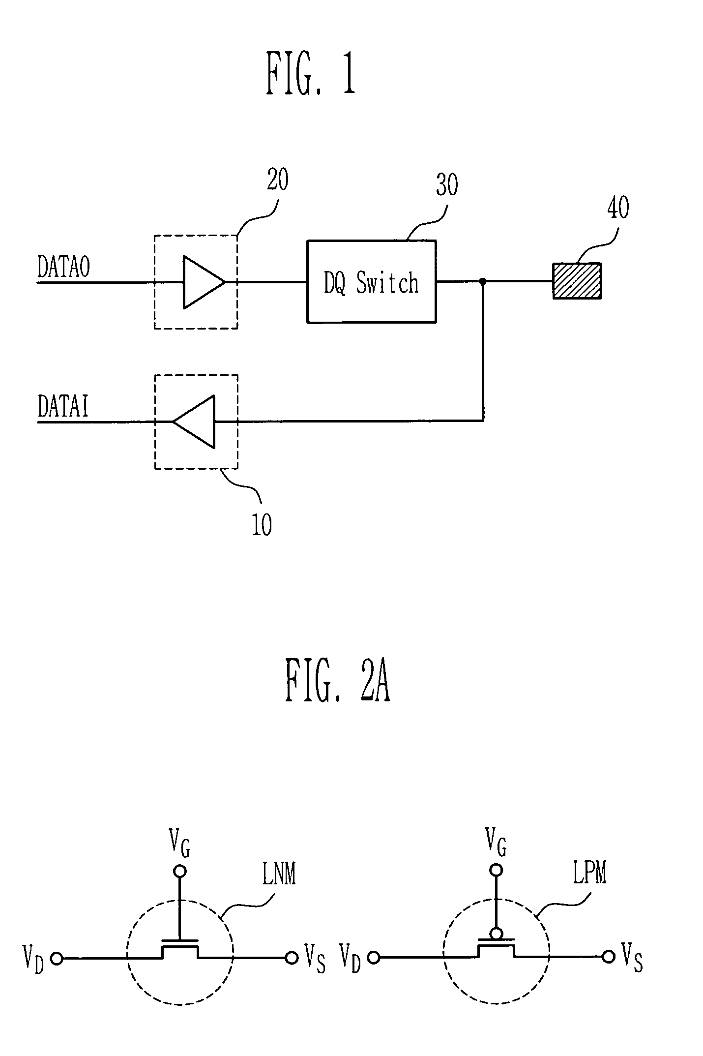
[0020]FIG. 1 is a block diagram of an input and output driver according to a preferred embodiment.

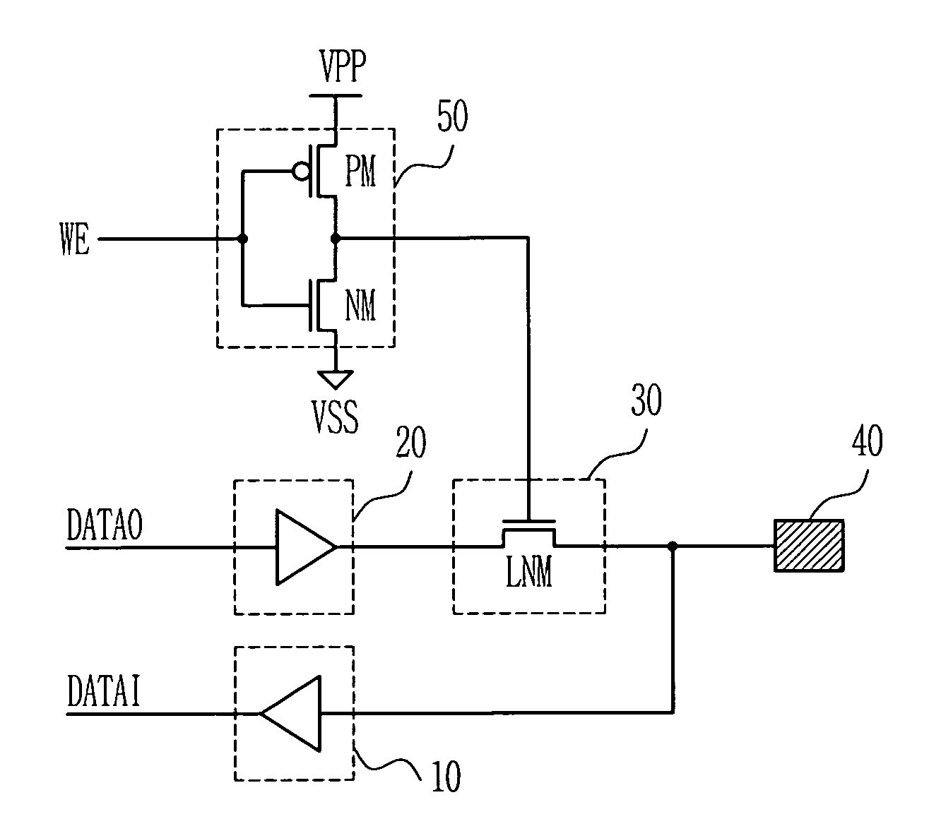
[0021]Referring to FIG. 1, an input and output driver according to a preferred embodiment comprises an input buffer 10, an output driver 20, and a DQ switch 30, and is connected to a DQ pad 40.

[0022]In a writing mode, the DQ switch 30 is turned-off to electrically isolate the output driver 20 from the DQ pad 40. On the other hand, in a reading mode, the DQ switch 30 is turned-on to electrically connect the output driver 20 to the DQ pad 40.

[0023]In the writing mode, the DQ switch 30 is tuned-off to electrically isolate the output driver 20 fro...


PUM


Abstract

An input and output driver is disclosed which includes comprising a DQ switch capable of reducing a total input capacitance Cin by electrically isolating an output driver from a DQ pad using the DQ switch in a writing mode to reduce the capacitance due to the output driver.

Description

BACKGROUND[0001]1. Technical Field[0002]The present invention relates to an input and output driver and, more specifically, to an input and output driver capable of effectively reducing an input capacitance (Cin) of a double data rate (DDR)-III product.[0003]2. Discussion of Related Art[0004]Double data rate (DDR)-III standard graphic DRAM products require a channel impedance of 40Ω in which at least 30Ω tuning is supported. Furthermore, an on-die termination (ODT) circuit, which is provided to match impedance between a graphic processor unit (GPU) and a graphic DRAM (GDRAM), requires impedance of about 60Ω. Furthermore, in the GDRAM, the input capacitance Cin is limited to 3 pF or less to insure transmission of signal wave forms at the time of high-speed operation of 700 MHz level.[0005]Generally, a DQ pin for transmitting and receiving data is connected to complex circuit elements, such as an input buffer, an output driver, an electrostatic discharge protection circuit (herein aft...

Claims


Application Information

Patent Timeline
Patent Type & Authority Patents(United States)
IPC IPC(8): H03K19/0175H03K19/00G11C7/10G11C11/4096
CPCG11C7/1051G11C7/1066G11C7/1069G11C7/1096G11C11/4096G11C7/1078G11C2207/105G11C7/10
Inventor LEE, CHANG YEOLGONG, MYEONG KOOK
Owner SK HYNIX INC
Why Eureka
Try Eureka