Lateral transient voltage suppressor with ultra low capacitance

a transient voltage and suppressor technology, applied in the direction of emergency protective circuit arrangements, emergency protective arrangements for limiting excess voltage/current, emergency protective arrangements, etc., can solve the problems of high input capacitance of traditional tvs, esd (electrostatic discharge) events, and the function of these electronics could be reset or even damaged under esd events, so as to reduce the input capacitance , the effect of low input capacitan

Active Publication Date: 2012-01-19
AMAZING MICROELECTRONICS
View PDF0 Cites 14 Cited by
  • Summary
  • Abstract
  • Description
  • Claims
  • Application Information

AI Technical Summary

Benefits of technology

[0008]A primary objective of the present invention is to provide a lateral transient voltage suppressor, which adopts deep isolation trenches to separate each doped well arranged in the substrate, so as to obtain the ultra low input capacitance. The ultra low input capacitance of the suppressor can not only benefit the signal performance but be achieved for high speed interface application.

Problems solved by technology

Without suitable protection devices, the functions of these electronics could be reset or even damaged under ESD (Electrostatic Discharge) events.
However, after well drive-in process, the dosage of the P-type lightly doped well 24 and the N-type lightly doped well 30 will be still affected by the P-type doped well 38 and increased, which results in high input capacitance of the traditional TVS.
However, the TVS device size should be designed large for better ESD performance which causes the large input capacitance.
Therefore, how to reduce input capacitance of TVS device without reducing device size is a challenge.

Method used


Image

  • Lateral transient voltage suppressor with ultra low capacitance
  • Lateral transient voltage suppressor with ultra low capacitance
  • Lateral transient voltage suppressor with ultra low capacitance

Examples


first embodiment

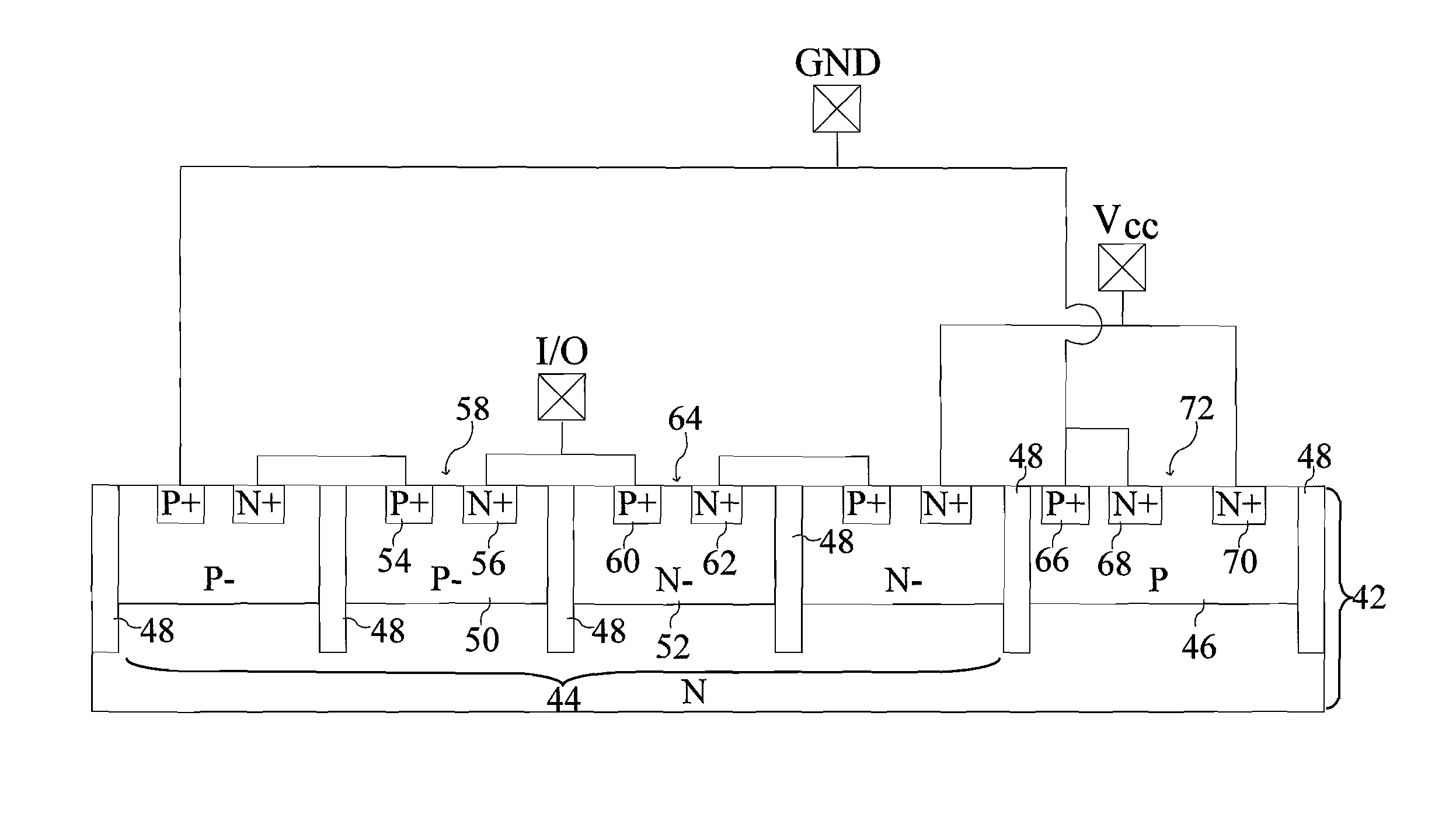
[0020]Refer to FIG. 4 and FIG. 5, wherein FIG. 5 is an equivalent circuit of FIG. 4. The transient voltage suppressor (TVS) of the present invention comprises a first type substrate 42. At least one diode cascade structure 44, a second type well 46, and a plurality of deep isolation trenches 48 are all arranged in the first substrate 42. The second type well 46 neighbors the diode cascade structure 44. For much reduced the input capacitance of the present invention, the diode cascade structure 44 comprises at least one second type lightly doped well 50 arranged in the first substrate 42 and at least one first type lightly doped well 52 arranged in the first substrate 42. In the first embodiment, the numbers of the diode cascade structure 44, the second type lightly doped well 50, and the first type lightly doped well 52 are all one, which is used as an example. And, for example, the first type substrate 42 is an N-type substrate, the second type well 46 is a P-type well, the second ...

third embodiment

[0030]In the third embodiment, the left most second type lightly doped well 50 is regarded as the first second type lightly doped well 50, and the most right first type lightly doped well 52 is regarded as the last first type lightly doped well 52. The first heavily doped area 54 of the first second type lightly doped well 50, the fifth and sixth heavily doped areas 66, and 68 are connected with the low voltage. Also, the fourth heavily doped area 62 of the last first type lightly doped well 52 and the seventh heavily doped area 70 are connected with the high voltage Vcc, whereby the first and second heavily doped areas 54 and 56 of the second type lightly doped wells 50, and the third and fourth heavily doped areas 60 and 62 of the first type lightly doped wells 52 are all biased.

[0031]A deep isolation trenches 48 located between the second type lightly doped well 50 and the first type lightly doped well 52 is adjacent to them. Besides, a deep isolation trench 48 located between th...


PUM


Abstract

A lateral transient voltage suppressor with ultra low capacitance is disclosed. The suppressor comprises a first type substrate and at least one diode cascade structure arranged in the first type substrate. The cascade structure further comprises at least one second type lightly doped well and at least one first type lightly doped well, wherein there are two heavily doped areas arranged in the second type lightly doped well and the first type lightly doped well. The cascade structure neighbors a second type well, wherein there are three heavily doped areas arranged in the second type well. The suppressor further comprises a plurality of deep isolation trenches arranged in the first type substrate and having a depth greater than depths of the second type lightly doped well, the second type well and the first type lightly doped well. Each doped well is isolated by trenches.

Description

BACKGROUND OF THE INVENTION[0001]1. Field of the Invention[0002]The present invention relates to a lateral transient voltage suppressor, particularly to a lateral transient voltage suppressor with ultra low capacitance.[0003]2. Description of the Related Art[0004]Because the IC device sizes have been shrunk to nanometer scale, the consumer electronics, like the laptop and mobile devices, have been designed to be much smaller than ever. Without suitable protection devices, the functions of these electronics could be reset or even damaged under ESD (Electrostatic Discharge) events. Currently, all consumer electronics are expected to pass the ESD test requirement of IEC 61000-4-2 standard. TVS (Transient Voltage Suppressor) is generally designed to bypass the ESD energy, so that the electronic systems can be prevented from ESD damages. The working principle of TVS is shown in FIG. 1. In FIG. 1, the TVS devices 10 are connected in parallel with the protected circuits 12 on the PCB (Prin...

Claims


Application Information

Patent Timeline
Patent Type & Authority Applications(United States)
IPC IPC(8): H01L29/06
CPCH01L27/0255
Inventor CHUANG, CHE-HAOLIN, KUN-HSIENJIANG, RYAN HSIN-CHIN
Owner AMAZING MICROELECTRONICS
Why Eureka
Try Eureka