Offset cancellation amplifier, display employing the offset cancellation amplifier and method for controlling the offset cancellation amplifier

a technology of offset cancellation amplifier and offset cancellation, which is applied in the direction of amplifiers, amplifiers with semiconductor devices/discharge tubes, electrical devices, etc., can solve the problems of increasing the effective input capacitance of the operational amplifier, and the accuracy of the output cannot be raised beyond a certain limit, so as to improve the output accuracy and output potential vout

Inactive Publication Date: 2007-08-30
NEC CORP
View PDF14 Cites 15 Cited by
  • Summary
  • Abstract
  • Description
  • Claims
  • Application Information

AI Technical Summary

Benefits of technology

[0039]During the horizontal period H2, only the voltage Vout2 at the output terminal may be varied. Hence, the voltage applied to the gate of the transistor M6 is Vout2, during the period T03, thus upsetting the drain c

Problems solved by technology

The aforementioned offset cancellation amplifier, shown in FIG. 16, for example, is of high accuracy, however, the accuracy in the output cannot be raised beyond a certain limit, because of variations in the potential retained by the capacitor C1 due to noise from the ground or to noise generated when

Method used


Image

  • Offset cancellation amplifier, display employing the offset cancellation amplifier and method for controlling the offset cancellation amplifier
  • Offset cancellation amplifier, display employing the offset cancellation amplifier and method for controlling the offset cancellation amplifier
  • Offset cancellation amplifier, display employing the offset cancellation amplifier and method for controlling the offset cancellation amplifier

Examples


first example

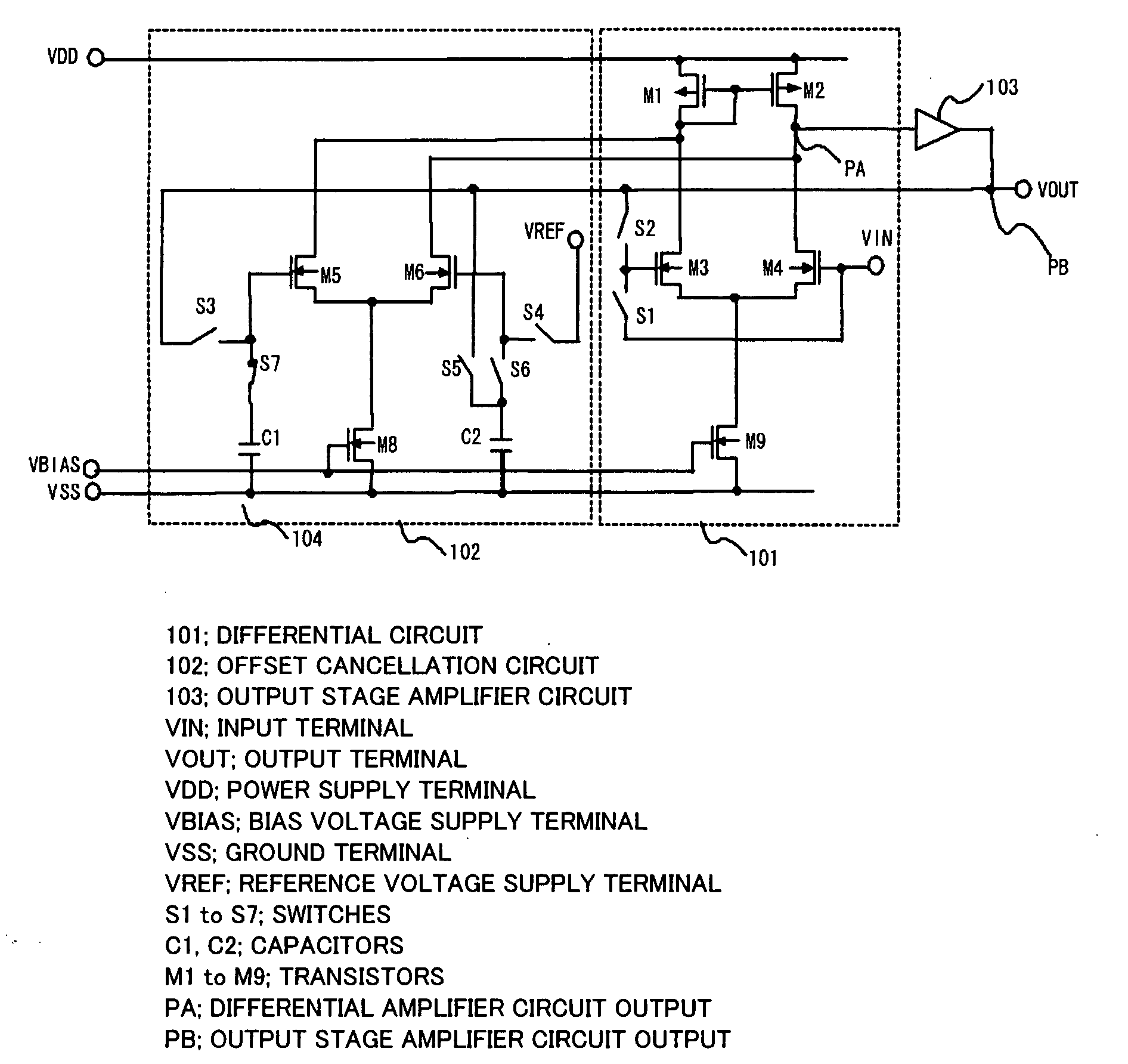
[0094]The circuit configuration of a first example of the present invention will now be described. FIG. 1 shows the configuration of a differential amplifier according to the present invention. Referring to FIG. 1, the differential amplifier of the present example includes:

[0095]NMOS transistors M5 and M6 having sources connected in common to form a differential pair;

[0096]NMOS transistors M3 and M4, having sources connected in common to form another differential pair;

[0097]an NMOS transistor M8 having a source connected to a power supply VSS, having a drain connected to the common source of the differential pair (M5, M6) and having a gate supplied with a bias voltage from a bias voltage supply terminal VBIAS to constitute a current source;

[0098]an NMOS transistor M9 having a source connected to the power supply VSS, having a drain connected to the common source of the differential pair (M3, M4) and having a gate supplied with a bias voltage from the bias voltage supply terminal VBI...

second example

[0125]The circuit configuration of the second example of the present invention will now be described. FIG. 4 shows the configuration of a differential amplifier of the second example of the present invention. In FIG. 4, the reference voltage supply terminal VREF in the circuit configuration of the first example in FIG. 1 is made the same as the input terminal VIN. That is, the point of difference of the present example from the first example shown in FIG. 1 resides in the connection to the switch S4. In the first example, the switch S4 is provided between the reference voltage supply terminal VREF and a connection point between the gate of the NMOS transistors M6 and the switch S6, whereas, in the configuration of FIG. 4, the switch S4 is provided between the input terminal VIN and a connection point between the gate of the NMOS transistor M6 and the switch S6. Hence, the reference voltage Vref is the input voltage Vin. The present example is otherwise the same as the example shown ...

third example

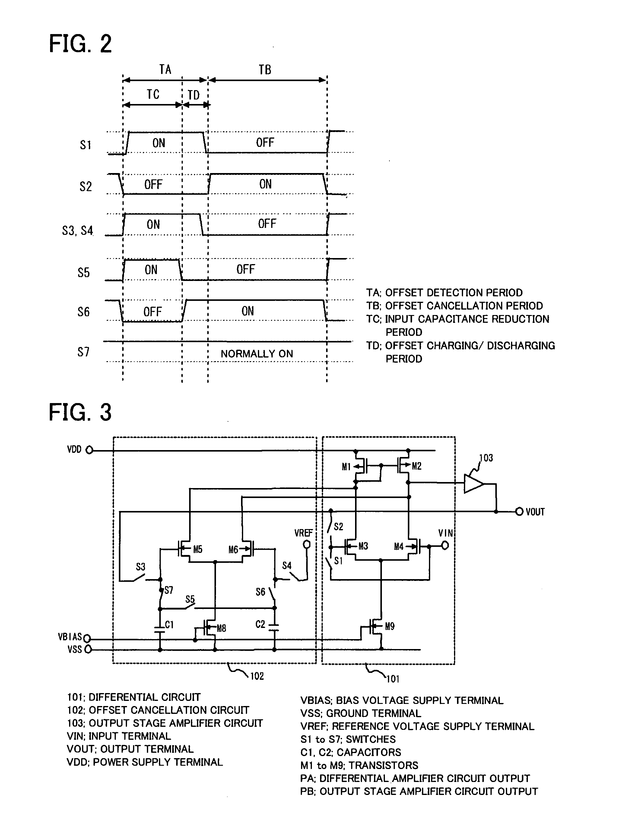
[0140]The circuit configuration of a third example of the present invention will now be described in detail. FIG. 5 shows the configuration of a differential amplifier according to a third example of the present invention. Meanwhile, the configuration of FIG. 5 differs from that of FIG. 4 as to the manner of switch control. The configuration of the present example suppresses the input capacitance from increasing and improves the slew rate to provide for a shorter offset detection period.

[0141]Referring to FIG. 5, showing the differential amplifier of the present example, a differential pair (M5, M6), driven by a current source (transistor M8 supplied with VBIAS) and a differential pair (M3, M4), driven by a current source (M9), are connected in common to a load circuit. In FIG. 5, the specified load circuit is composed of a transistor M1, connected in a diode configuration, and a transistor M2, having a gate connected to a gate of M1.

[0142]The gate of one M5 of the transistors of th...


PUM


Abstract

Disclosed is an offset cancellation amplifier which includes a first differential pair, second differential pair, a common load circuit for the two differential pairs, current sources, an amplifier stage, and first and second capacitors. The first capacitor is connected to the gate of one transistor of the first differential pair. During a first period of a data output period, an output voltage and the reference voltage are supplied to the gates of the first differential pair, the second capacitor is disconnected from the gate of the other transistor of the first differential pair. In this state, the output voltage is accumulated in the first and second capacitors. An input voltage is supplied in common to the gates of the second differential pair During the second period, the second capacitor is disconnected from the first capacitor and connected to the gate of the other transistor of the first differential pair. The output voltage is accumulated in the first capacitor, while the reference voltage is accumulated in the second capacitor. During the third period, the gates of the first differential pair cease to be supplied with the output voltage and with the reference voltage, respectively, and are supplied with the voltages accumulated in the first and second capacitors, respectively. The gates of the second differential pair are supplied with the output voltage and with the input voltage, respectively.

Description

FIELD OF THE INVENTION[0001]This invention relates to an offset cancellation amplifier, in particular, an offset cancellation amplifier adapted for suppressing the effect of noise and which is provided with a circuit for reducing input capacitance. This invention also relates to a method for controlling the offset cancellation amplifier.BACKGROUND OF THE INVENTION[0002]In a liquid crystal display, an operational amplifier has been in use as an amplifier in driving a load on a data line. For example, an operational amplifier shown in FIG. 13 comprises a differential amplifier 901 and an output stage amplifier circuit 903. Of these, the differential amplifier 901 includes a differential pair, composed of NMOS transistors M3 and M4, having sources connected in common, and an active load circuit, which is a current mirror. This current mirror is composed of a PMOS transistor M1, having a source connected to a power supply VDD (high side power supply or positive power supply) and having ...

Claims


Application Information

Patent Timeline
IPC IPC(8): H03F1/02
CPCH03F3/45183H03F3/45753H03F3/45762H03F2200/453H03F2203/45726H03F2203/45588H03F2203/45616H03F2203/45652H03F2203/45681H03F2203/45212
Inventor IRIGUCHI, MASAO
Owner NEC CORP
Why Eureka
Try Eureka