Insulating barrier, NVM bandgap design

a technology of insulating barrier and band gap, which is applied in the direction of transistors, nanotechnology, electrical devices, etc., can solve the problems of compromising long-term data retention, difficult to construct barriers, and aln is not a suitable material for constructing such barriers, so as to reduce energy barriers, increase dielectric constant, and strengthen voltage dependence

Inactive Publication Date: 2006-04-11
INTERUNIVERSITAIR MICRO ELECTRONICS CENT (IMEC VZW)
View PDF4 Cites 10 Cited by
  • Summary
  • Abstract
  • Description
  • Claims
  • Application Information

AI Technical Summary

Benefits of technology

[0008]The insulating barrier according to one aspect of the invention comprises a first portion contacting the first region and a second portion contacting the first portion and extending towards the second region. The first portion is substantially thinner than the second portion. The first portion is constructed in a first dielectric and the second portion in a second dielectric which differs from and has a higher dielectric constant than the first dielectric. Due to the higher dielectric constant of the second portion, the first portion will have a larger voltage drop than the second portion when a voltage is applied over the insulating barrier. In other words, the electric field over the first portion will be stronger than the electric field over the second portion. As a result, the energy band diagram over the first portion has a stronger voltage dependence than the energy band diagram over the second portion, i.e. the energy band diagram upon applying a suitable voltage for tunnelling will show a steeper inclination over the first portion than over the second portion. In this way, less tunnelling voltage is required with respect to the single-layer insulating barrier of the prior art in order to reduce the energy barrier during tunnelling by the same amount. Furthermore, as the first portion is substantially thinner than the second portion, the profile during tunnelling comprises a larger part with the more shallow inclination, which implies that the tunnelling voltage can be reduced by a substantial amount with respect to the single-layer insulating barrier.
[0009]Suitable material combinations for the insulating barrier of the invention are for example SiO2 or Si3N4 for the first portion and Al2O3, HfO2 or ZrO2 for the second portion. The second portion can for example be deposited by a technique such as atomic layer chemical vapour deposition (ALCVD), which can easily be achieved. Furthermore, Al2O3, HfO2 and ZrO2 are high-barrier materials which are currently considered for use in standard silicon semiconductor technology, for example in the standard CMOS transistor process, in contrary to the AlN which is used in the barrier of U.S. Pat. No. 6,121,654 and is not a commonly used or considered material in silicon technology. As a result, the insulating barrier of the invention can be constructed more easily, as the use of additional materials which are not already used in the normal transistor manufacturing process can be avoided. Of course, any other material combinations which are deemed suitable to the person skilled in the art may also be used in the insulating barrier of the invention.
[0011]Preferably, the material and the thicknesses of the first and second portions are chosen such that, upon applying a voltage suitable for tunnelling over the insulating barrier, the voltage drop over the first portion is higher than the voltage drop over the second portion. This has the advantage that the largest part of the tunnelling voltage will be dropped over the first portion, which is substantially thinner than the second portion. As a result, the tunnelling voltage can be further reduced.
[0014]In the first preferred embodiment, the dielectrics of the three portions are preferably chosen such that, in absence of a voltage difference over the insulating barrier, the three portions have substantially the same potential energy barrier. This has the advantage that the energy band diagram does not comprise any steps, so that during tunnelling the diagram descends monotonously. In this way it can be achieved that the second portion during tunnelling does not form an additional barrier, as is for example the case with the insulating barrier of U.S. Pat. No. 6,121,654 (see FIG. 6). Furthermore, this implies that, in absence of a voltage difference over the insulating barrier, the first and third portions provide an additional energy barrier to the energy barrier which is formed by the second portion, as the potential energy level of the first and third portions is sufficiently high to avoid electrons travelling to the first and third portions by thermionic emission, which can for example occur in the first and third layers of the insulating barrier of U.S. Pat. No. 6,121,654 which have a lower potential energy barrier than the second (interposed) layer. As a result, the thickness of the second portion can be reduced in the insulating barrier of the invention with respect to the insulating barrier known from U.S. Pat. No. 6,121,654.
[0015]In a second preferred embodiment of the invention, the insulating barrier comprises first and second portions of which the dielectrics are chosen such that, in absence of a voltage difference over the insulating barrier, the first portion has a higher potential energy barrier than the second portion. In other words, the energy band diagram of the insulating barrier has a stepped profile with a higher step over the first portion than over the second portion. This has the advantage that the voltage dependence of the insulating barrier can be further increased, as the profile comprises a vertically descending part between the first and second portions. This enables direct tunnelling instead of Fowler-Nordheim tunnelling through the first portion. In this way, the voltage which is required for tunnelling can be further reduced. This second embodiment also has the advantage that the energy band diagram during tunnelling descends monotonously, with the same advantages as mentioned in respect of the first embodiment described above.

Problems solved by technology

However, the insulating barrier described in U.S. Pat. No. 6,121,654 has the disadvantage that such a barrier cannot easily be constructed, as there are only few suitable material combinations, and that all of these combinations have practical problems.
However, Si3N4 does not have the required ordered structure and therefore the structure of the AlN layer that is deposited on a Si3N4 layer will have defects that can compromise the long term data retention.
Hence AlN is not a suitable material for constructing such an insulating barrier.

Method used


Image

  • Insulating barrier, NVM bandgap design
  • Insulating barrier, NVM bandgap design
  • Insulating barrier, NVM bandgap design

Examples


first embodiment

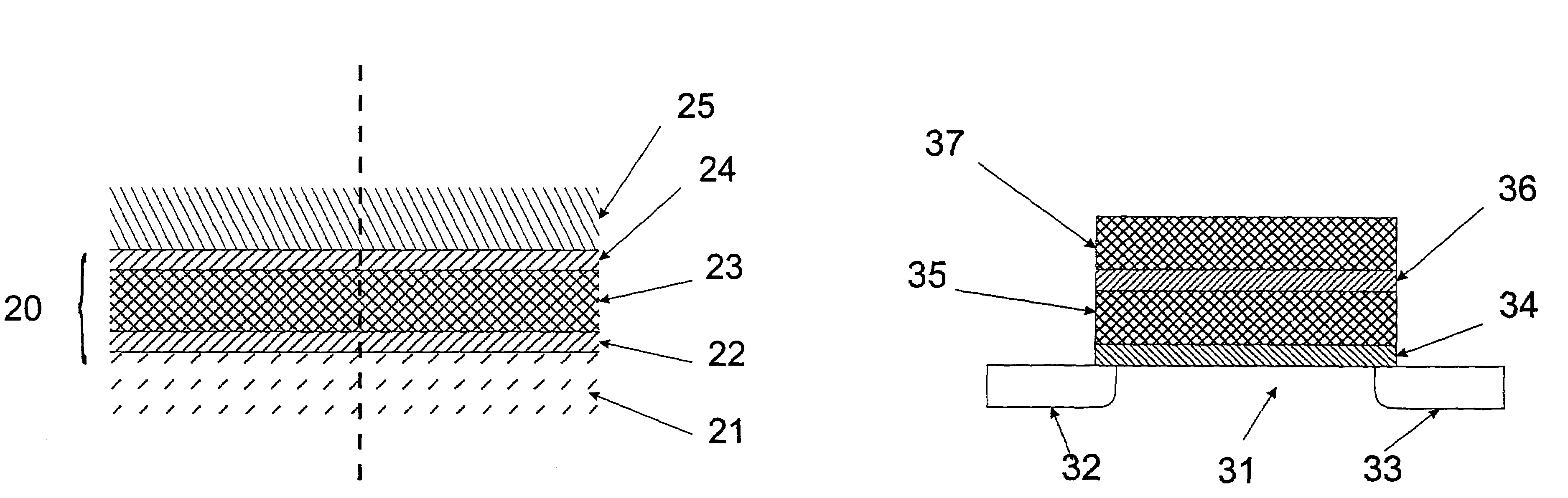
[0040]Referring to FIG. 7, there is shown the insulating barrier. The insulating barrier 20 extends between a first conductive region 21 and a second conductive region 25 and comprises first, second and third layers 22, 23 and 24, which are formed on top of each other. The first and third layers 22 and 24 are preferably constructed in a first dielectric material having a low dielectric constant. The second layer 23 is substantially wider than the first and third layers 22 and 24 and is constructed in a second dielectric material having a higher dielectric constant than the first dielectric material.

[0041]The first and second dielectric materials are chosen such that the insulating barrier 20 has a energy band diagram as shown in FIG. 8, when no voltage is applied over the barrier, and as shown in FIG. 9, when the tunnelling voltage is applied over the barrier. In order to achieve the profile shown in FIG. 8, the first and second dielectric materials are chosen such that they have su...

second embodiment

[0074]Referring to FIGS. 18, 19 and 20, a third memory device is shown. In this memory cell, the writing is done by means of hot electron injection, such as is for example known from the HIMOS™ cell which is described in U.S. Pat. No. 5,583,810. However, the interpoly dielectric between the control gate 57 and the floating gate 55 of the HIMOS™ cell is replaced by an insulating barrier 56 according to the invention as shown in FIG. 11, with the first layer 22 of dielectric material having a high dielectric constant contacting the floating gate 55. This replacement leads to a certain number of important improvements in the operation of the memory cell of FIGS. 18, 19 and 20 with respect to the HIMOS™ cell.

[0075]The erasing of the HIMOS™ cell is done by tunnelling of the charge carriers between floating gate and control gate. This tunnelling can either be Fowler-Nordheim tunnelling or tunnelling through a polyoxide where asperities of the underlying layer enhance the electric field an...


PUM


Abstract

An insulating barrier extending between a first conductive region and a second conductive region is disclosed. The insulating barrier is provided for tunnelling charge carriers from the first to the second region, the insulating barrier comprising a first portion contacting the first region and a second portion contacting the first portion and extending towards the second region, the first portion being substantially thinner than the second portion, the first portion being constructed in a first dielectric and the second portion being constructed in a second dielectric different from the first dielectric, the first dielectric having a lower dielectric constant than the second dielectric.

Description

CROSS REFERENCE TO RELATED APPLICATIONS[0001]This application is a continuation of U.S. patent application Ser. No. 10 / 131,923, filed on Apr. 25, 2002 U.S. Pat No. 6,784,484 which claims priority benefits to United States provisional application Ser. No. 60 / 287,192, filed on Apr. 27, 2001, entitled “Insulating Barrier.” Application Ser. No. 10 / 131,923 also claims priority to European Patent Application EP 01204106.7 filed on Oct. 19, 2001. This application incorporates by reference U.S. application Ser. No. 10 / 131,923 and provisional application Ser. No. 60 / 287,192 in their entirety. This application also incorporates by reference European Patent Application EP 01204106.7 in its entirety.FIELD OF THE INVENTION[0002]The present invention relates to an insulating barrier provided for tunnelling electrons from a first conductive region to a second conductive region according to the preamble of the first claim.BACKGROUND OF THE INVENTION[0003]Such an insulating barrier is for example us...

Claims


Application Information

Patent Timeline
Patent Type & Authority Patents(United States)
IPC IPC(8): H01L29/792H01L21/28H01L29/51H01L29/788
CPCB82Y10/00H01L21/28194H01L21/28273H01L29/792H01L29/517H01L29/518H01L29/7883H01L29/7885H01L29/513H01L21/28202H01L29/40114
Inventor BLOMME, PIETERGOVOREANU, BOGDANROSMEULEN, MAARTEN
Owner INTERUNIVERSITAIR MICRO ELECTRONICS CENT (IMEC VZW)
Why Eureka
Try Eureka