Molded package for micromechanical devices and method of fabrication

a micromechanical device and molded package technology, applied in the direction of semiconductor devices, semiconductor/solid-state device details, electrical apparatus, etc., can solve the problems of high overall package structure and low package cost of today's micromechanical device and manufacturing method

Inactive Publication Date: 2006-04-11
TEXAS INSTR INC
View PDF36 Cites 50 Cited by
  • Summary
  • Abstract
  • Description
  • Claims
  • Application Information

AI Technical Summary

Benefits of technology

[0012]It is an aspect of the present invention to be applicable to a variety of different semiconductor micromechanical devices, for instance actuators, motors, sensors, spatial light modulators, and deformable mirror devices. In all applications, the invention achieves technical advantages as well as significant cost reduction and yield increase.
[0014]It is another aspect of the present invention to modify the transfer molding technique so that it becomes applicable to encapsulating micromechanical devices and concurrently protects the micromechnical components during the total process (for example against dust and released chemicals), resulting in significantly higher manufacturing yield and enhanced device quality and reliability.
[0019]Another aspect of the invention is to provide flexibility of the package structure relative to the geometry (contour and area) of the semiconductor chip containing the plurality of micromechanical components.

Problems solved by technology

Today's overall package structure for micromechnical devices and method of fabrication is expensive.
This fact is in conflict with the market requirements for many applications of micromechanical devices, which put a premium at low device cost and, therefore, low package cost.

Method used


Image

  • Molded package for micromechanical devices and method of fabrication
  • Molded package for micromechanical devices and method of fabrication
  • Molded package for micromechanical devices and method of fabrication

Examples


Embodiment Construction

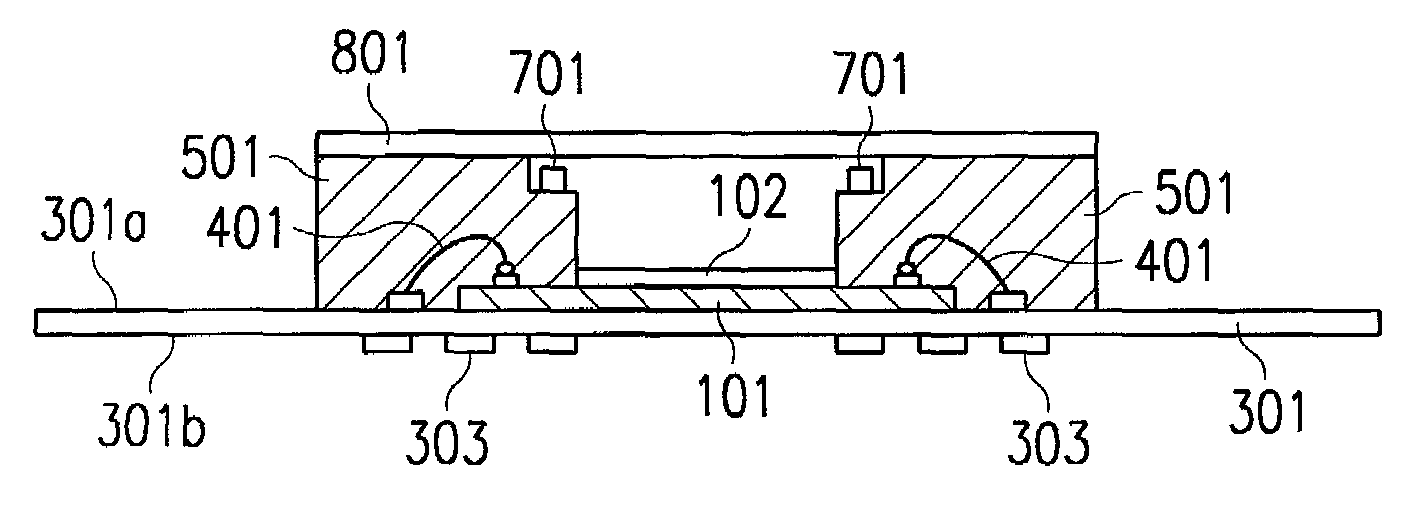
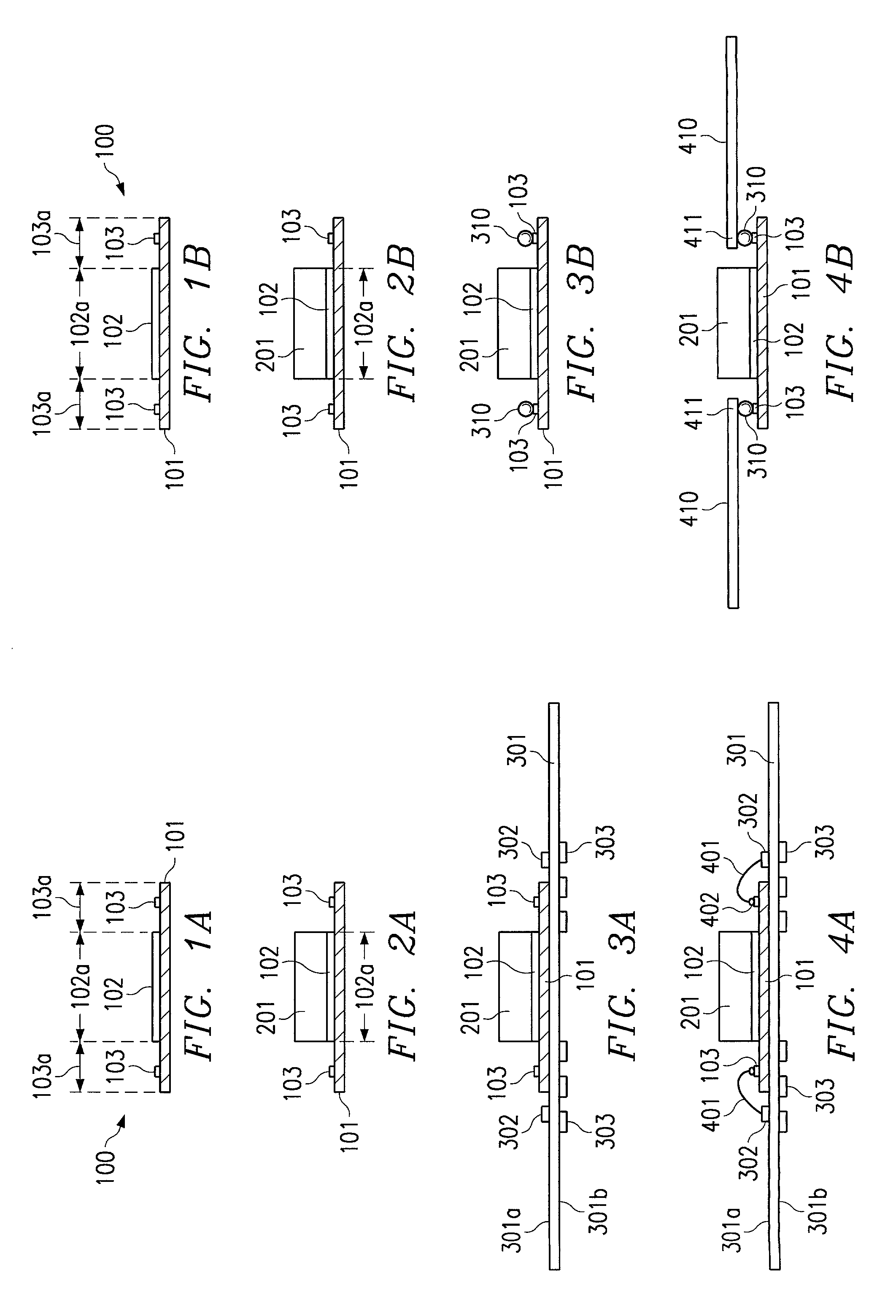
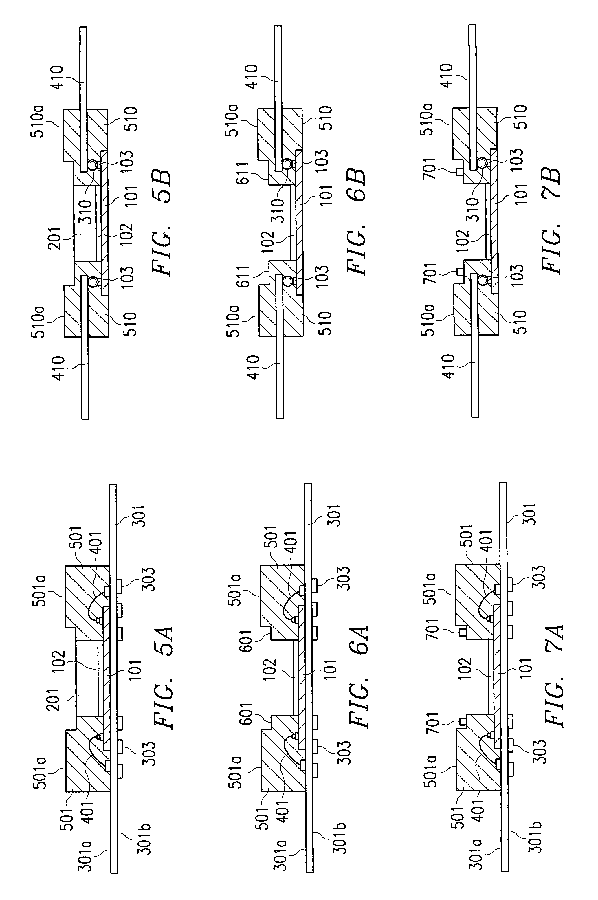
[0045]In FIGS. 1A and 1B, a semiconductor chip of the micromechanical type is shown, generally designate 100. Chip 100 is formed on and in a single-crystalline material 101, typically silicon; it includes an integrated circuit (not shown) and a plurality of micromechanical components 102 in the central area 102a of the chip. The micromechanical components are disposed in a plane. Further, chip 100 includes a plurality of bonding pads 103 as input / output terminals of the integrated circuit and the micromechanical components. The bonding pads are disposed in the peripheral areas 103a of the chip.

[0046]As mentioned above, the micromechanical components 102 may include actuators, motors, sensors, spatial light modulators, and deformable mirror devices. By way of example and purposes of illustration, micromechanical components 102 are digital micromirror devices (DMD), as manufactured by Texas Instruments Incorporated of Dallas, Tex., U.S.A.

[0047]Structures and methods of micromechanical...


PUM


Abstract

According to the present invention, a plastic land-grid array package, a plastic ball-grid package, and a plastic leaded package for micromechanical components are fabricated by a molding process characterized by placing a sheet-like protector on the surface of the components during the molding phase, selectively encapsulating the bonding pads and coupling members of the chip while leaving empty space above the components, removing the protector and attaching a lid over the components. A molding method as well as a molding apparatus are provided compatible with the sensitivity of the micromechanical devices, yet flexible with regard to the technique used to assemble the chip and the substrate. Furthermore, the method disclosed is flexible with regard to the material and the properties of the substrate. The invention is applicable to a variety of different semiconductor micromechanical devices, for instance actuators, motors, sensors, spatial light modulators, and deformable mirror devices. In a key embodiment of the invention, the micromechanical components are micromirrors for a digital mirror device.

Description

[0001]This application claims priority under 35 USC § 119 based upon Provisional Patent Application No. 60 / 177,446 filed Jan. 21, 2000.FIELD OF THE INVENTION[0002]The present invention is related in general to the field of semiconductor devices and processes and more specifically to the design and fabrication of a molded package generally for micromechanical devices and specifically for digital mirror devices.DESCRIPTION OF THE RELATED ART[0003]Micromechanical devices include actuators, motors, sensors, spatial light modulators (SLM), digital micromirror devices or deformable mirror devices (DMD), and others. The technical potential of these devices is especially evident when the devices are integrated with semiconductor circuitry using the miniaturization capability of semiconductor technology.[0004]SLMs are transducers that modulate incident light in a special pattern pursuant to an electrical or other input. The incident light may be modulated in phase, intensity, polarization or...

Claims


Application Information

Patent Timeline
Patent Type & Authority Patents(United States)
IPC IPC(8): H01L23/12
CPCB81C1/00333H01L2224/45147H01L2924/01047H01L2924/1815H01L2924/15311H01L2224/48227H01L2224/48091H01L2224/16245H01L2924/10253H01L2924/00014H01L2924/00H01L2224/45015H01L2224/05573H01L2224/05568H01L2224/05624H01L2224/05644H01L2224/05647H01L24/45H01L2924/181H01L2224/0554H01L2924/207H01L2224/05599H01L2224/0555H01L2224/0556
Inventor COYLE, ANTHONY L.BEDNARZ, GEORGE A.
Owner TEXAS INSTR INC
Why Eureka
Try Eureka