Solid-state image pickup device

Inactive Publication Date: 2006-04-18
RENESAS ELECTRONICS CORP
View PDF16 Cites 80 Cited by
  • Summary
  • Abstract
  • Description
  • Claims
  • Application Information

AI Technical Summary

Benefits of technology

[0037]It is preferable the light shielding layer is composed of a single layer or plural layers that have a sufficient light tightness with low light transparency or high light absorbency, and it may be formed of an organic material such as gelatin or casein, or it may be formed of a material with reduced light transparency or limited wavelength of transmitted light obtained by mixing a pigment or the l

Problems solved by technology

Consequently, according to such a structure of the CMOS sensor, false signals generated by the photoelectric conversion effect of the light incident on the periphery of the photoelectric conversion region 14 leaks into adjacent photoelectric conversion region, and causes the problem of degradation of the S/N of image signals.
However, in such a case, the quantity of light incident on the photoelectric conversion region 14 is reduced, and results in the problem of the reduction in the sensitivity.
This leads to the problem of

Method used


Image

  • Solid-state image pickup device
  • Solid-state image pickup device
  • Solid-state image pickup device

Examples


first embodiment

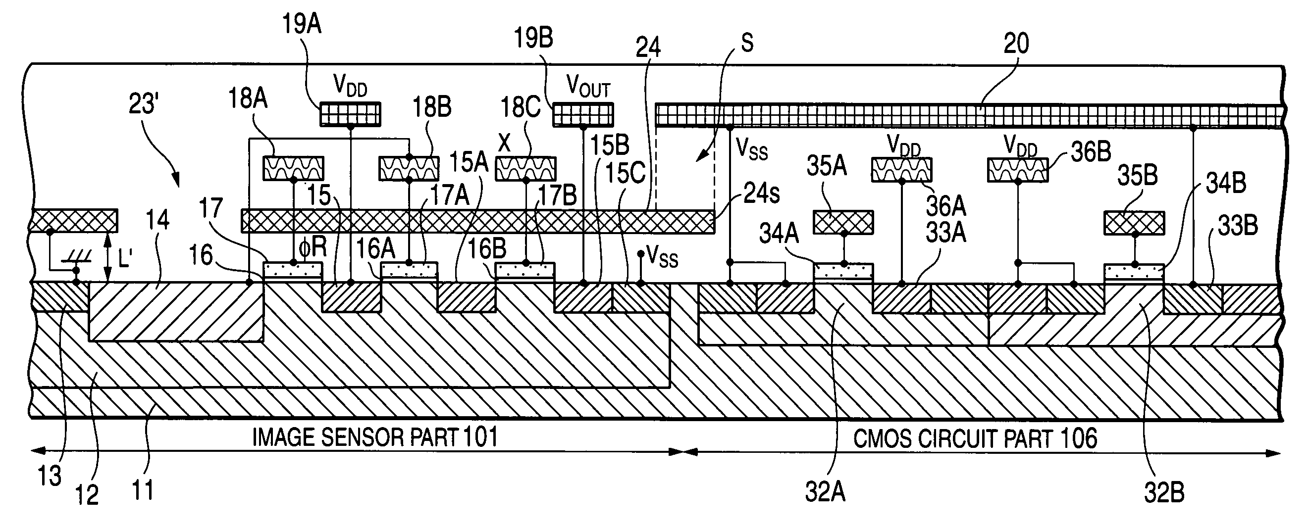
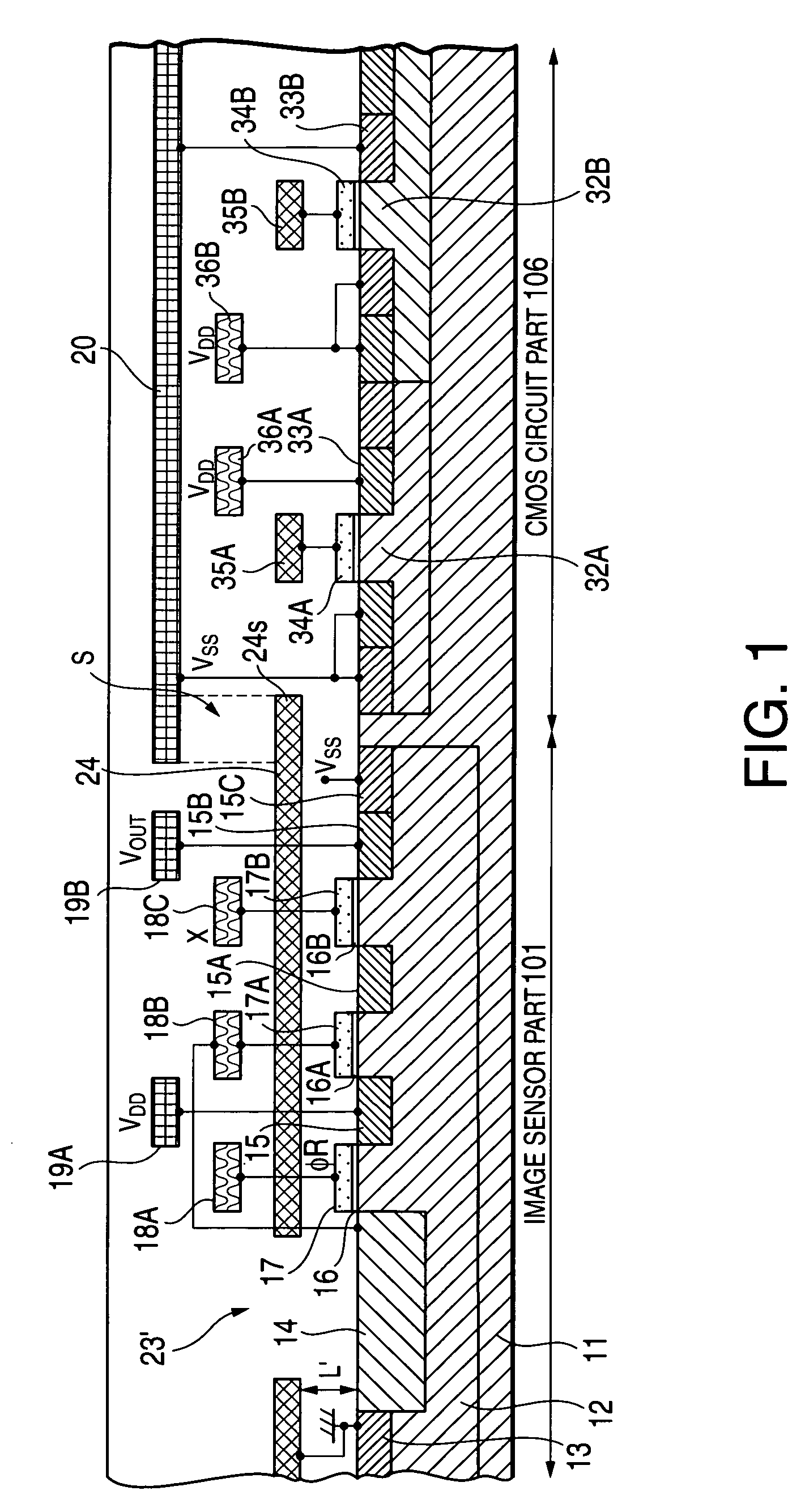
[0054]Next, referring to the drawings, the solid-state image pickup device according to this invention will be described.

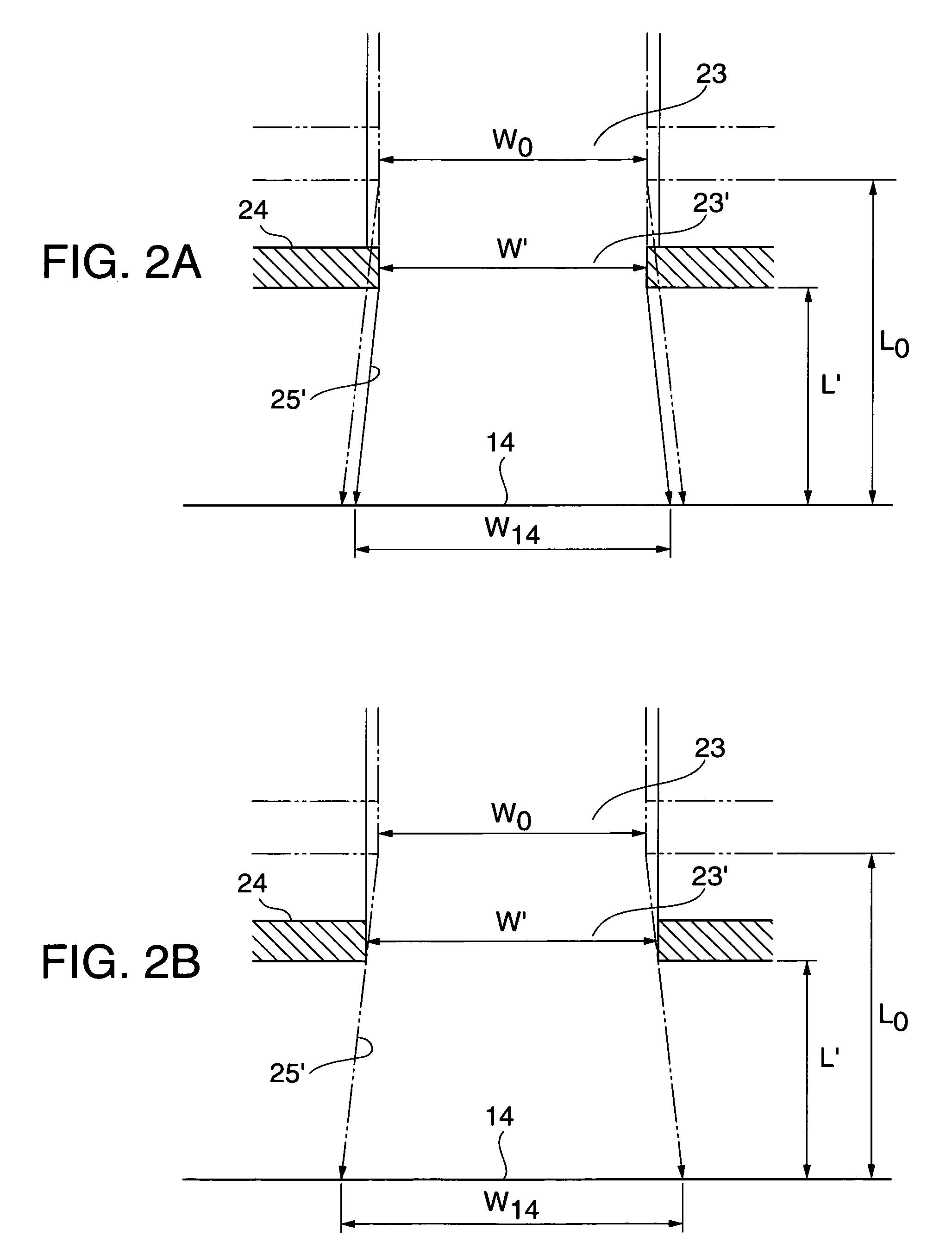
[0055]FIG. 1 is a schematic side view showing the solid-state image pickup device according to this embodiment, and FIGS. 2A and 2B are schematic enlarged side views showing the photoelectric conversion region and the light shielding film.

[0056]The solid-state image pickup device in this embodiment is assumed to be an active XY address type CMOS sensor 100 similar to that as shown in FIG. 12.

[0057]Such a CMOS sensor 100 is provided with an image sensor part (photoelectric conversion part) 101 in which several hundreds several hundreds of fundamental cells are arranged to deal with the pixels, a timing generating part 102, a vertical scanning part 103 and a horizontal scanning part 104 for selecting pixel outputs, an analog signal processing part 105, an A / D part (A / D conversion part) 109 which performs analog to digital conversion of signals, a digital signal proc...

second embodiment

[0112]Next, the solid-state image pickup device according to this invention will be described.

[0113]FIG. 7 is a schematic side view showing the solid-state image pickup device of the present embodiment.

[0114]In this embodiment, the difference from the first embodiment shown in FIG. 1 and FIG. 2 consists in the point relating to the light shielding film and the wiring layers in the image sensor part, where the constituent elements approximately the same as in the first embodiment shown in FIG. 1 to FIG. 6 are given the same symbols.

[0115]In the solid-state image pickup device in this embodiment, the light shielding film 24 is provided closer to the semiconductor substrate 11 than the light shielding layer 20 as shown in FIG. 7, and it is composed of a plurality of parts 24A and 24B.

[0116]The light shielding films 24A and 24B are provided at different heights, and their boundary part of each of them is provided with an overlapping part S. The overlapping part S is given a configuratio...

third embodiment

[0126]Next, referring to the drawings, the solid-state image pickup device according to this invention will be described.

[0127]In FIG. 9, which shows a schematic side view of the solid-state image pickup device according to the present embodiment, symbols 20A, 20B, and 20C are light shielding layers of this embodiment and 20D is a color filter.

[0128]In this embodiment, the difference from the first and second embodiments shown in FIG. 1 to FIG. 8 relates to the light shielding layer 20.

[0129]In the embodiment, the light shielding layer positioned at the topmost layer of the logic circuit part 106 consists of a plurality of layers 20A, 20B, and 20C that are laminated to cover the entirety of the logic circuit part 106, where these light shielding layers have insulating property, and have low light transparency or high light absorbency and sufficient light shielding property.

[0130]Here, it is preferable that the light shielding layers 20A, 20B, and 20C have either low light transparen...


PUM


Abstract

The present invention discloses a solid-state image pickup device in which a photoelectric conversion part having a photoelectric conversion region, and a logic circuit part are formed on a semiconductor substrate, and outputs a potential change caused by the charges generated in the photoelectric conversion region, and is provided with a light shielding layer that covers the logic circuit part, and a light shielding film that defines the region of beam incidence on the photoelectric conversion region, where the light shielding film is provided closer to the semiconductor substrate than the light shielding layer.

Description

BACKGROUND OF THE INVENTION[0001]1. Field of the Invention[0002]The present invention relates to a solid-state image pickup device, and more particularly to a technology adapted to an active XY address type solid-state image pickup device among solid-state image pickup devices compatible with the CMOS manufacturing processes (the so-called CMOS sensors) or to a CCD sensor.[0003]2. Description of the Prior Art[0004]The conventional solid-state image pickup devices of the transfer layer type that transfer photoelectrically converted signal charges can roughly be classified into those of MOS type and CCD type. These solid-state image pickup devices, especially the solid-state image pickup devices of the CCD type, have been applied in recent years to camera-integrated VTRs, digital cameras, facsimile equipment, and the like, and are still in the process of technical development for improvement of their characteristics.[0005]A CCD sensor is equipped with a photoelectric conversion part i...

Claims


Application Information

Patent Timeline
IPC IPC(8): H04N3/14H01L27/00H01L31/112H01L31/113H04N5/228H01L23/60H01L27/14H01L27/146H01L27/148H04N5/335H04N5/357H04N5/369H04N5/372H04N5/3745
CPCH01L27/14621H01L27/14623H01L27/14636H01L2924/0002H01L2924/00H01L27/146
Inventor NAKASHIBA, YASUTAKA
Owner RENESAS ELECTRONICS CORP
Why Eureka
Try Eureka