

Image forming device
a technology of image forming and forming bias, which is applied in the direction of electrographic process apparatus, instruments, optics, etc., can solve the problems of excessive discharge current decrease in the resistance of the contact transfer body, etc., and achieve the effect of avoiding the continuation of the conventional overdischarge condition, high degree of quality, and applying time of the transfer cleaning bias
- Summary
- Abstract
- Description
- Claims
- Application Information
AI Technical Summary
Benefits of technology
Problems solved by technology
Method used
Image

Examples
Embodiment Construction
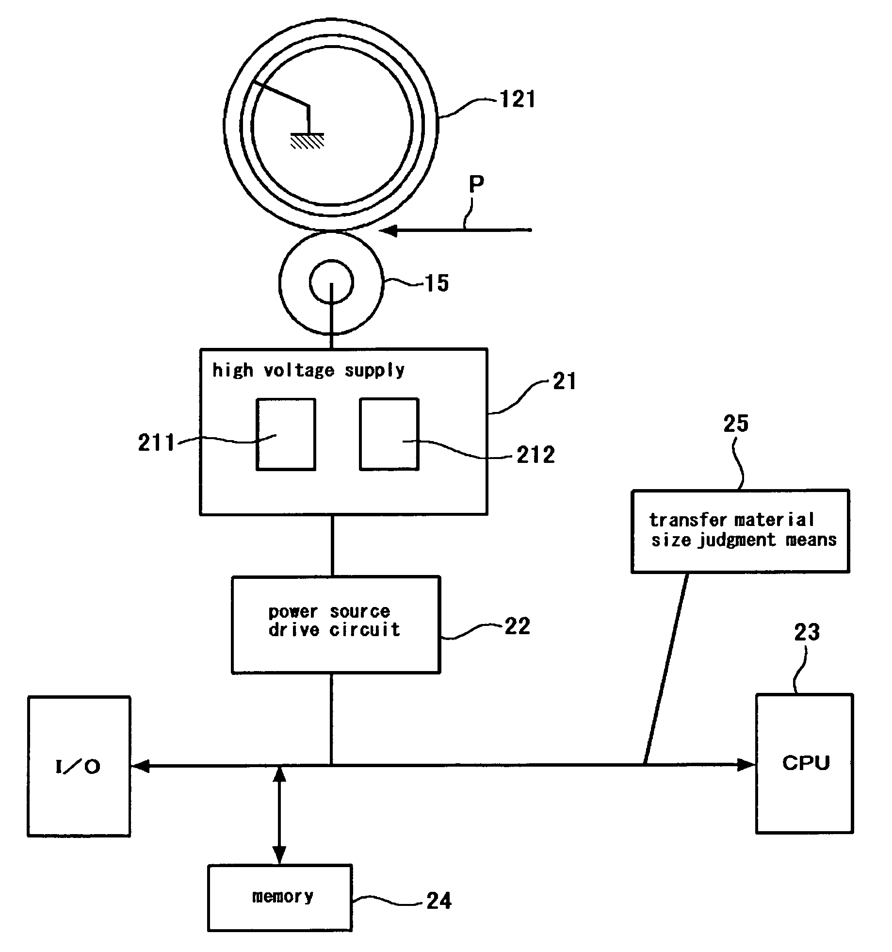
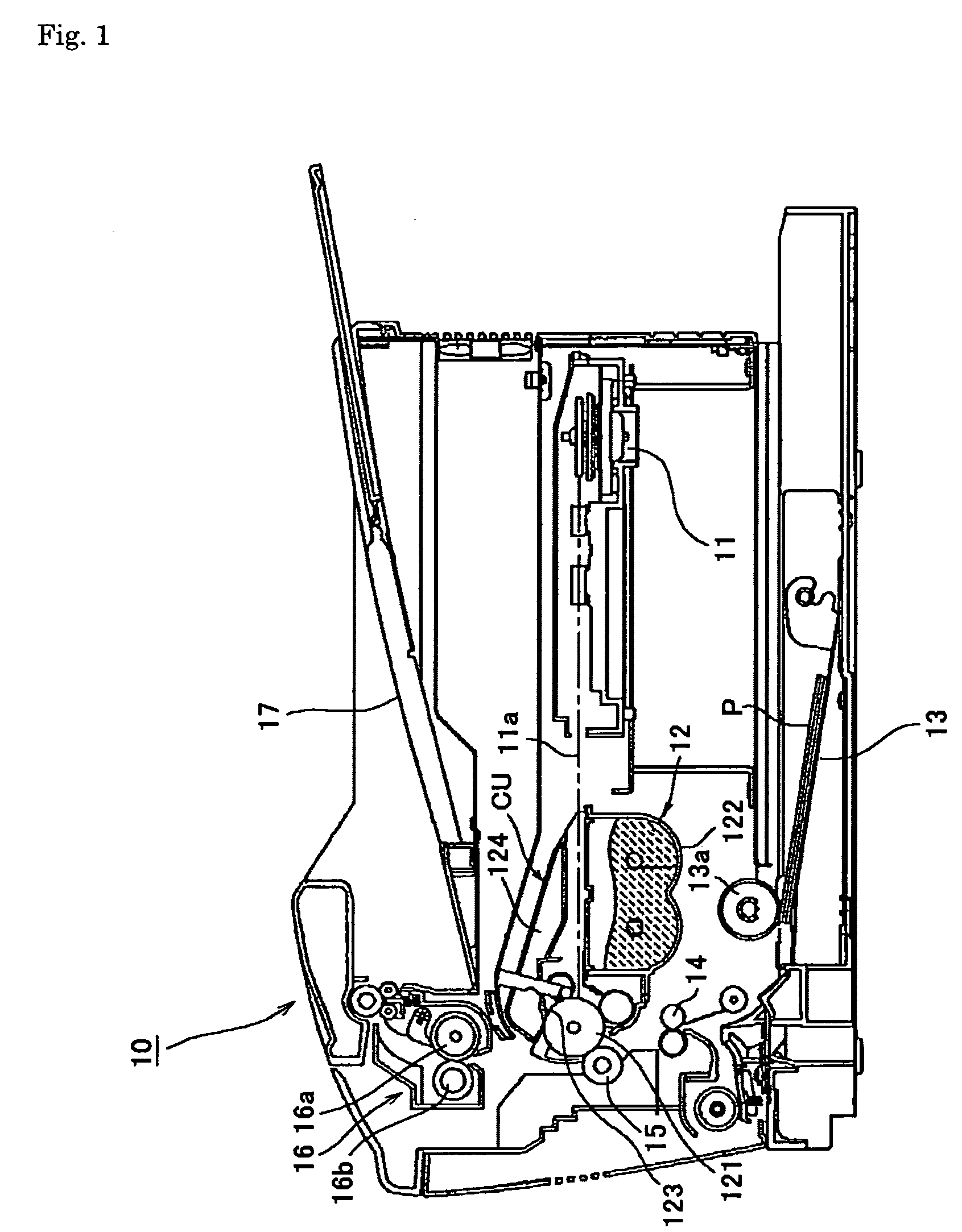
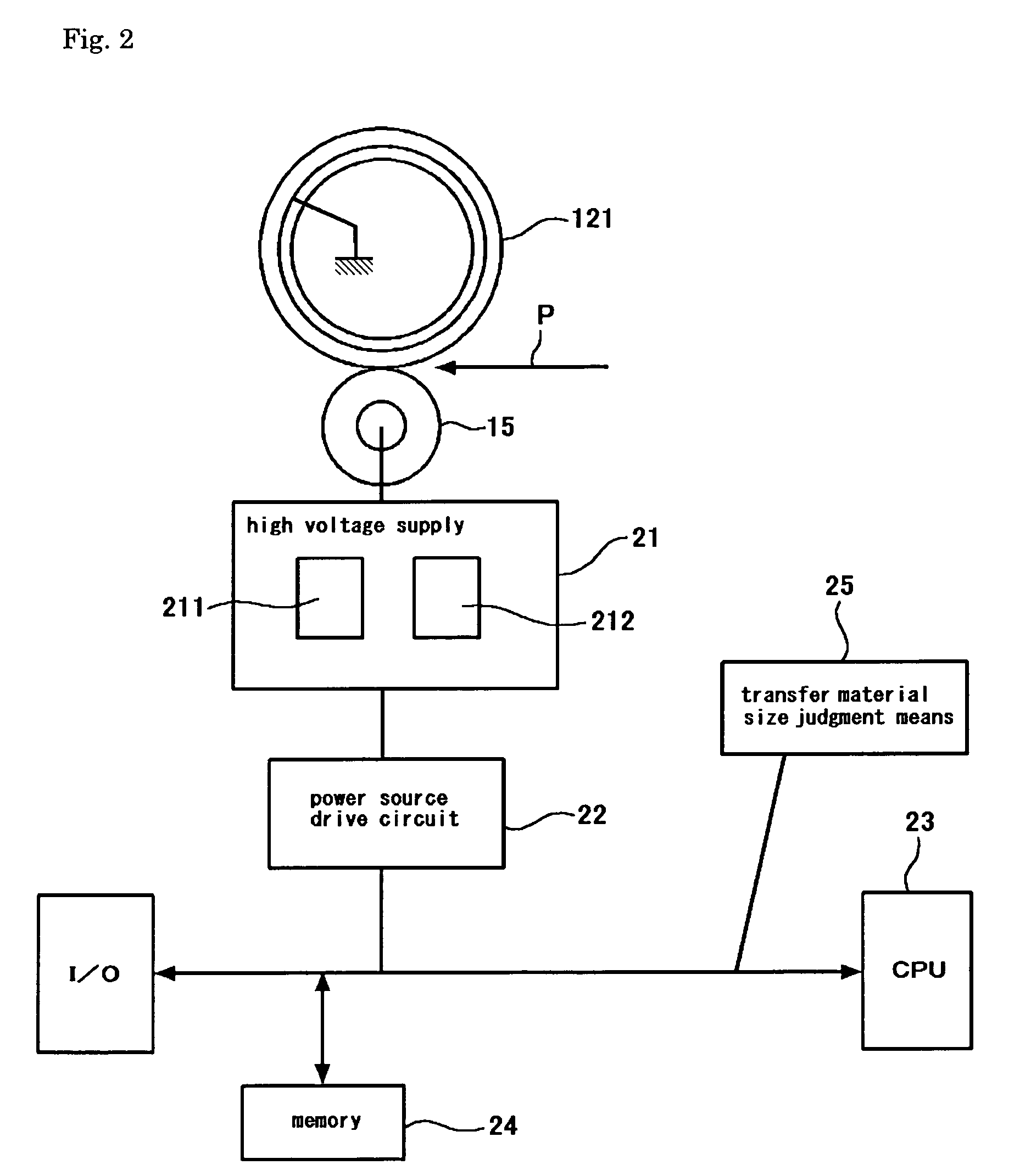
[0023]An embodiment of the present invention will be described in detail below with reference to the accompanying drawings. A schematic description of a laser printer will be made first as an example of the entire constitution of an image forming device.
[0024]In a laser printer 10 shown in FIG. 1, image information sent from an external computer is focused as optically-modulated information 11a in a spot shape on a photosensitive drum 121 as an image carrier by a laser emission writing part 11, which is installed in a process cartridge 12, by using a video controller not shown in the drawing. The optical spot is reciprocally scanned in the axial direction (main scanning direction) of the photosensitive drum 121 and an electrostatic latent image is formed on the photosensitive drum 121 so as to correspond to the image to be formed. A developer (toner) is supplied from a developing unit 122 integrally provided within the process cartridge 12 to an electrostatic latent image on the pho...
PUM
 Abstract
Description
Claims
Application Information