Apparatus and method for testing defects

a technology of defect testing and apparatus, applied in semiconductor/solid-state device testing/measurement, therapy, instruments, etc., can solve the problems of poor insulation, poor insulation of capacitors, and destruction of typically gate oxide films,

Inactive Publication Date: 2006-05-02
HITACHI HIGH-TECH CORP
View PDF53 Cites 43 Cited by
  • Summary
  • Abstract
  • Description
  • Claims
  • Application Information

AI Technical Summary

Benefits of technology

[0017]It is another object of the present invention to provide a defect inspecting apparatus and a defect inspection method which allow a high-efficiency substrate fabrication line to be constructed by implementation of complete inspection and sampling inspection at a sufficiently high frequency.
[0060]Furthermore, in the configurations described above, it is possible to construct a high-efficiency substrate fabrication line by implementation of complete inspection and sampling inspection at a sufficiently high frequency.

Problems solved by technology

In the conventional semiconductor fabrication method, a foreign particle existing on a semiconductor substrate also known as a wafer causes a defect such as poor insulation of a wire or a short circuit.
Furthermore, in the case of a miniaturized semiconductor device, an infinitesimal foreign particle existing in a semiconductor substrate results in poor insulation of a capacitor or destruction of typically a gate oxide film.
Likewise, if a foreign particle is introduced to get mixed with a pattern, causing some defects in a process to fabricate a liquid-crystal display device, the resulting display device is not usable.
In addition, publications 1 to 8 also have a problem of a substantially reduced sensitivity in the case of an oxide film which passes a radiation beam.
Moreover, publications 1 to 8 also have a problem of inability to detect a defect such as an infinitesimal foreign particle.
At any rate, the conventional defect inspecting apparatus is large in size and has such a configuration that the apparatus must be installed independently.
As a result, complete inspection is difficult.
In addition, it is hard to carry out such sampling inspection at a sufficiently high frequency.
Further, a defect inspecting apparatus with such a configuration requires an operator.

Method used


Image

  • Apparatus and method for testing defects
  • Apparatus and method for testing defects
  • Apparatus and method for testing defects

Examples


first embodiment

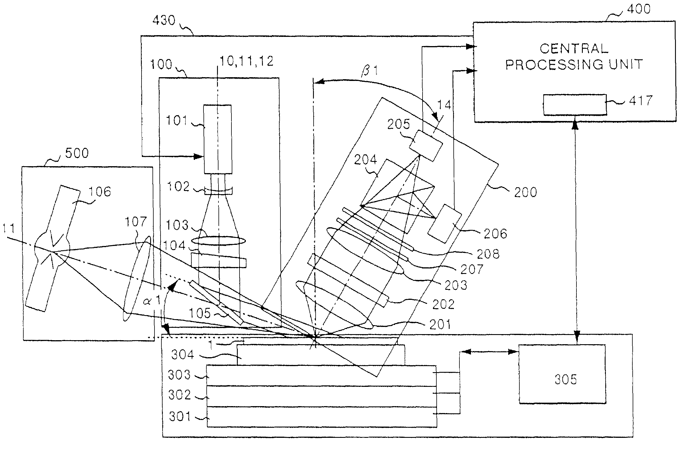
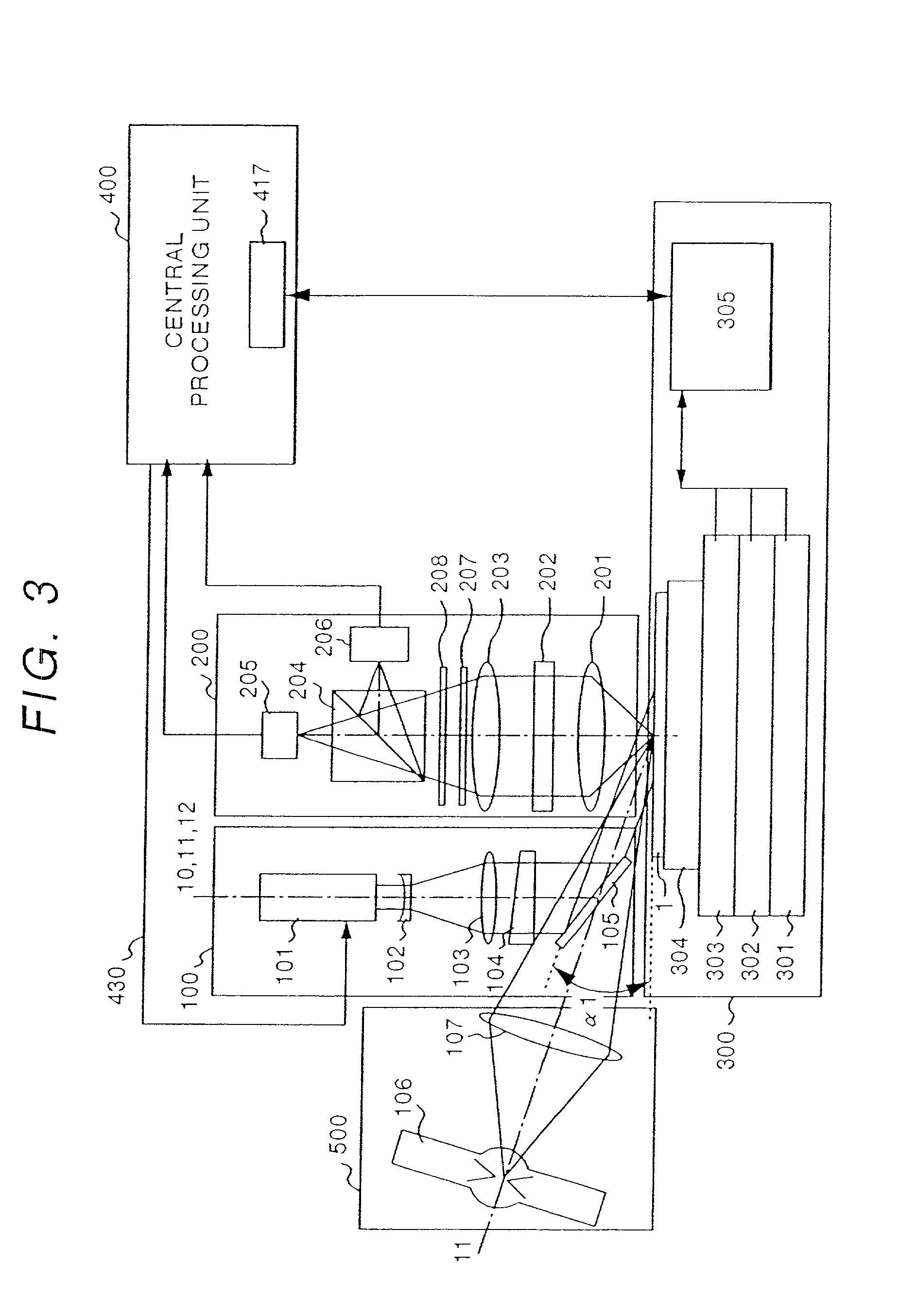
[0120]The following description explains a first embodiment implementing a defect inspecting apparatus provided by the present invention to detect a defect such as a foreign particle by referring to FIGS. 3 and 4.

[0121]As shown in FIG. 3, the first embodiment implementing a defect inspecting apparatus for detecting a defect such as a foreign particle comprises: a stage unit 300 comprising a substrate mounting base 304, x, y and z stages 301, 302 and 303 and a stage controller 305; 3 illumination optical systems 100 having a laser-beam source 101, a beam splitter comprising a concave lens 102 and a convex lens 103 and an illumination lens 104 having a conical surface; a detection optical system 200 including a detection lens 201, a spatial filter 202, an image formation lens 203, an ND (Neutral Density) filter 207, a beam splitter 204, a polarization device 208 and one-dimensional detectors (image sensors) 205 and 206 which are each implemented typically by a TDI image sensor; an ima...

second embodiment

[0160]If TDI (Time Delay Integration) sensors are used as the detectors 205 and 206, however, the optical axis of the detection optical system 200 can not be inclined due to a focal depth. Thus, in the case of the second embodiment, one-dimensional sensors are employed. As an alternative, the magnification of a set comprising the detection lens 201, the spatial filter 202 and the image formation lens 203 employed in the detection optical system 200 is doubled or increased by several times and, as shown in FIG. 17, the TDI image sensors 205 and 206 are inclined at a gradient β2 expressed by Eq. (4) below. In this way, the magnification can be adjusted for the entire surface.

tan β2=M×tan β1  (4)

where the symbol M denotes the magnification of the set comprising the detection lens 201, the spatial filter 202 and the image formation lens 203.

[0161]It should be noted that, if one-dimensional sensors are employed, the inclination at the gradient β2 is not required.

[0162]The next descriptio...

fourth embodiment

[0188]The next description explains a fourth embodiment implementing a defect inspecting apparatus provided by the present invention for detecting a defect such as a foreign particle. By the way, with semiconductor devices miniaturized more and more, a further increase in yield is also required. To put it in detail, a circuit pattern created on a semiconductor substrate such as a semiconductor wafer for making such semiconductor devices is subjected to super miniaturization with a design rule of 0.3 to 0.2 μm or even smaller. For this reason, a foreign particle existing on the semiconductor substrate causes a semiconductor device created on the substrate to operate abnormally even if the foreign particle is an infinitesimal molecule with a size of about 0.1 μm or smaller or a particle with a size close to that at an atomic level.

[0189]In such a state of the art to fabricate a semiconductor device, the defect inspecting apparatus provided by the present invention for detecting a defe...


PUM

PropertyMeasurementUnit
angleaaaaaaaaaa
sizeaaaaaaaaaa
widthaaaaaaaaaa

Abstract

A defect inspection method includes radiating an illumination slit-shaped beam having lights substantially parallel to a longitudinal direction to a substrate having circuit patterns in a direction inclined at a predetermined gradient relative to the direction of a line normal to the substrate and inclined at a predetermined gradient on a surface with respect to a group of main straight lines of the circuit patterns with its longitudinal direction oriented almost perpendicularly to a direction of a movement of the substrate. Scattered light reflected by a defect such as a foreign particle existing on the illuminated substrate is received and converted into a detection signal by using an image sensor, and defect judging is effected of an extracted a signal indicating a defect such as a foreign particle on the basis of the detection signal output.

Description

CROSS-REFERENCE TO RELATED APPLICATIONS[0001]This is a continuation of U.S. application Ser. No. 09 / 362,135, filed Jul. 28, 1999, now U.S. Pat. No. 6,411,377, which is a continuation-in-part of U.S. application Ser. No. 08 / 535,577, filed Sep. 28, 1995, which is a continuation application of U.S. application Ser. No. 08 / 046,720, filed Apr. 16, 1993, now U.S. Pat. No. 5,463,459, which is a continuation-in-part of U.S. application Ser. No. 07 / 679,317, filed Apr. 2, 1991, now U.S. Pat. No. 5,233,191 and U.S. application Ser. No.07 / 778,363, filed Oct. 17, 1991, now U.S. Pat. No. 5,274,434.BACKGROUND OF THE INVENTION[0002]The present invention relates to a defect testing apparatus and a defect testing method for inspecting a state of generation of defects such as foreign particles in a fabrication process such as a semiconductor fabrication process, a liquid-crystal-display fabrication process and a print-board fabrication process wherein a defect such as a foreign particle generated in a...

Claims


Application Information

Patent Timeline
Patent Type & Authority Patents(United States)
IPC IPC(8): H01L21/66G01R31/26G01N21/94G01N21/95G01N21/956G01R31/308H01J37/00H01L21/00H01L21/68
CPCB82Y15/00G01N21/94G01N21/95623G01N21/95684G01R31/308H01J37/00H01L21/67253H01L21/67288H01L21/681H01L2924/0002G01N2021/8822H01J2237/022H01J2237/0225H01L22/12H01L2924/00
Inventor NOGUCHI, MINORIOHSHIMA, YOSHIMASANISHIYAMA, HIDETOSHIMATSUMOTO, SHUNICHIKEMBO, YUKIOMATSUNAGA, RYOUJISAKAI, KEIJININOMIYA, TAKANORIWATANABE, TETSUYANAKAMURA, HISATOJINGU, TAKAHIROMORISHIGE, YOSHIOCHIKAMATSU, SHUICHI
Owner HITACHI HIGH-TECH CORP
Why Eureka
Try Eureka