Backside contamination inspection device

a contamination inspection and backside technology, applied in the field of backside contamination inspection devices, can solve the problems of excessive amount of time required for inspection, the flipping process of the semiconductor wafer had a tendency to contaminate the edges of the wafer, and the front side of the wafer could be contaminated by the flipping process, so as to reduce the chance of contamination, reduce the opportunity for edge contamination, and effectively double the throughput of inspection equipmen

Inactive Publication Date: 2006-05-02
KLA CORP
View PDF10 Cites 10 Cited by
  • Summary
  • Abstract
  • Description
  • Claims
  • Application Information

AI Technical Summary

Benefits of technology

[0016]In the present invention, a semiconductor wafer is supported such that the semiconductor wafer lays flat during the inspection process. The surface is large enough to accommodate the wafer as well as the rollers for rotating the wafer and the means for holding the wafer. The wafer is preferably supported in a tilted or semi-upright orientation such that support is provided by gravity. This tilted supporting orientation permits both the frontside and the backside of the wafer to be viewed simultaneously by a frontside inspection device and a backside inspection device. The backside of the wafer for purposes of this invention is the side of the semiconductor wafer by which the wafer is being supported. Simultaneous dual-side inspection of the front side and back side of the wafer effectively doubles the throughput of inspection equipment and eliminates the need to turn the semiconductor wafer over during the inspection process, thereby reducing the opportunity for edge contamination of the inspected wafer.
[0017]The wafer is rotated by multiple motor-driven roller bearings. These drive rollers are positioned at the circumference of the wafer and are angled such that the roller pads contact the wafer only along the beveled edge. This periphery positioning and rotation coupled with angular contact between the rollers and wafer edge and surface permits inspection of the entire surface and significantly reduces the potential for contamination of the surface resulting from edge contact, or contact with the roller pads.
[0018]The drive rollers are spaced apart such that at least one of the two drive rollers spaced farthest apart contacts the round edge of the wafer throughout the rotation cycle. This constant contact feature ensures that the rotation rate of the wafer is suitably steady during defect inspection. Also, the steady rotation rate minimizes the number of defects missed or falsely detected by the inspection system.
[0019]The wafer rotation rate is such that roller contact does not damage the wafer edge. Furthermore, defects are not carried or transported from one part of the edge to another. Moreover, the rate should be controlled so as to minimize slip between the roller and the wafer edge. The present invention is intended for use at wafer rotation rates on the order of 400 revolutions per minute. Unlike previous systems, the present invention does not exhibit excessive vibration for defect inspection purposes at these rotation rates. The increased wafer rotation rate also increases the throughput of inspection equipment.
[0020]The semiconductor wafer is held against the drive rollers by pressure using a set of undriven roller bearings (contact rollers) or alternatively simply using gravitational force by tilting the wafer and inspection surface. This pressure ensures that the drive rollers hold traction on the beveled wafer edge so that a steady rotation rate can be maintained. All contact rollers thereby maintain contact with the edge of the semiconductor wafer throughout the rotation cycle.

Problems solved by technology

In addition to this excessive amount of time required for examination, the process of flipping the semiconductor wafer had a tendency to contaminate the edges of the wafer due to surface or edge contact with a gripping device.
In some processes, when the wafer was flipped over to inspect the backside, the front side of the wafer could be contaminated by the flipping process.
The resulting contamination of the frontside of the wafer tends to render the wafer unsuitable for further processing.
Thus, all test wafers were usually scrapped after each inspection, reducing overall productivity and increasing per unit cost.
Edge handling of wafers has also complicated the problem.
As wafers tend to suffer from contamination or other degradation when handled by wafer orientation systems, the handling of a wafer requires special care.
Systems without multiple drive rollers and radially inwardly-biased or spring-loaded contact rollers cannot maintain steady wafer rotation rate during the portion of a cycle in which the drive roller is not in contact with the round edge of the wafer because the drive roller loses traction along the wafer edge.
Previous systems which supported semiconductor wafers through direct contact with a solid surface present special problems during inspection since contact with the support surface may increase contamination or move defects from one location to another in ways that render the wafer unsuitable for future processing.

Method used


Image

  • Backside contamination inspection device
  • Backside contamination inspection device
  • Backside contamination inspection device

Examples


Embodiment Construction

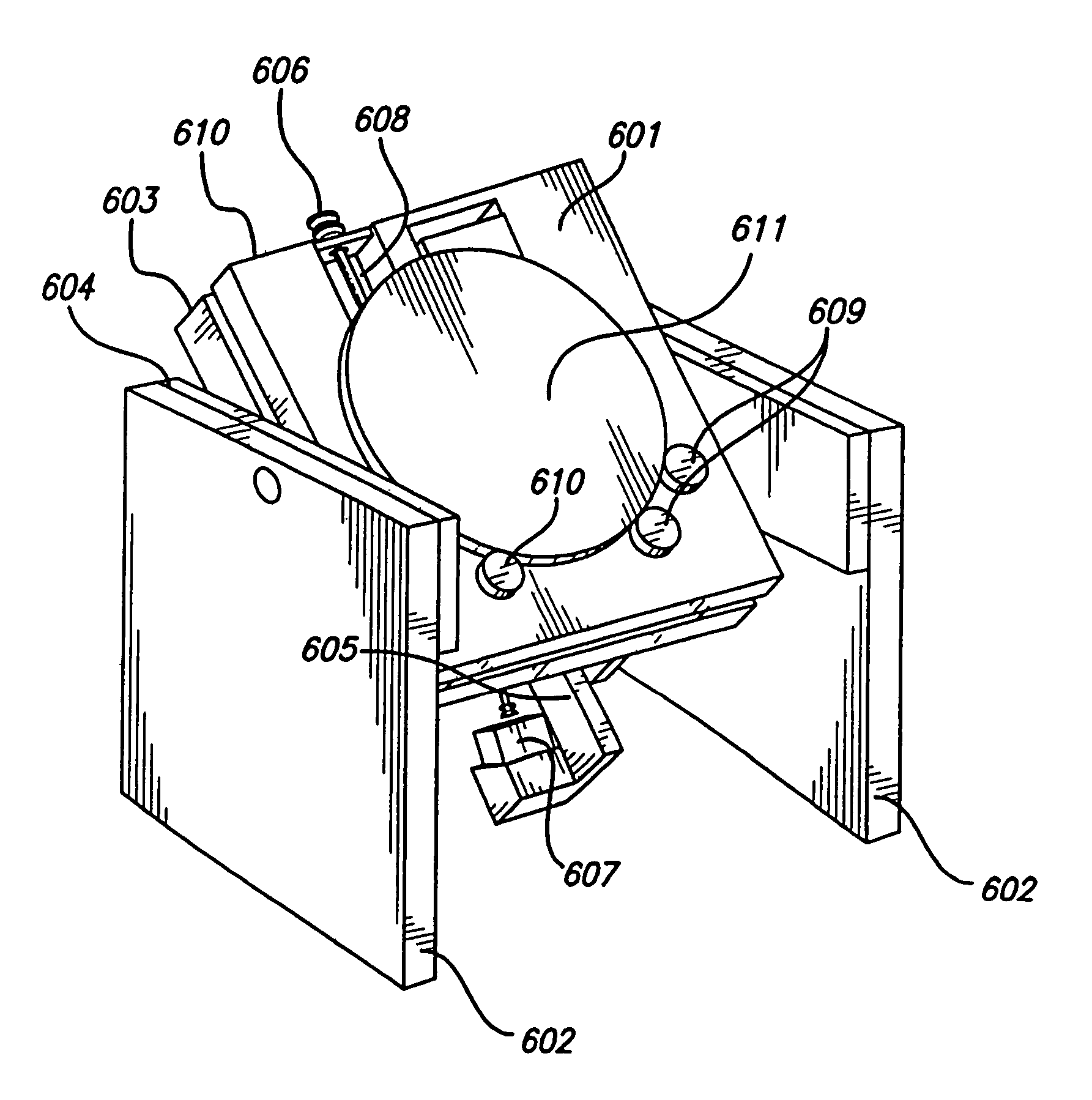
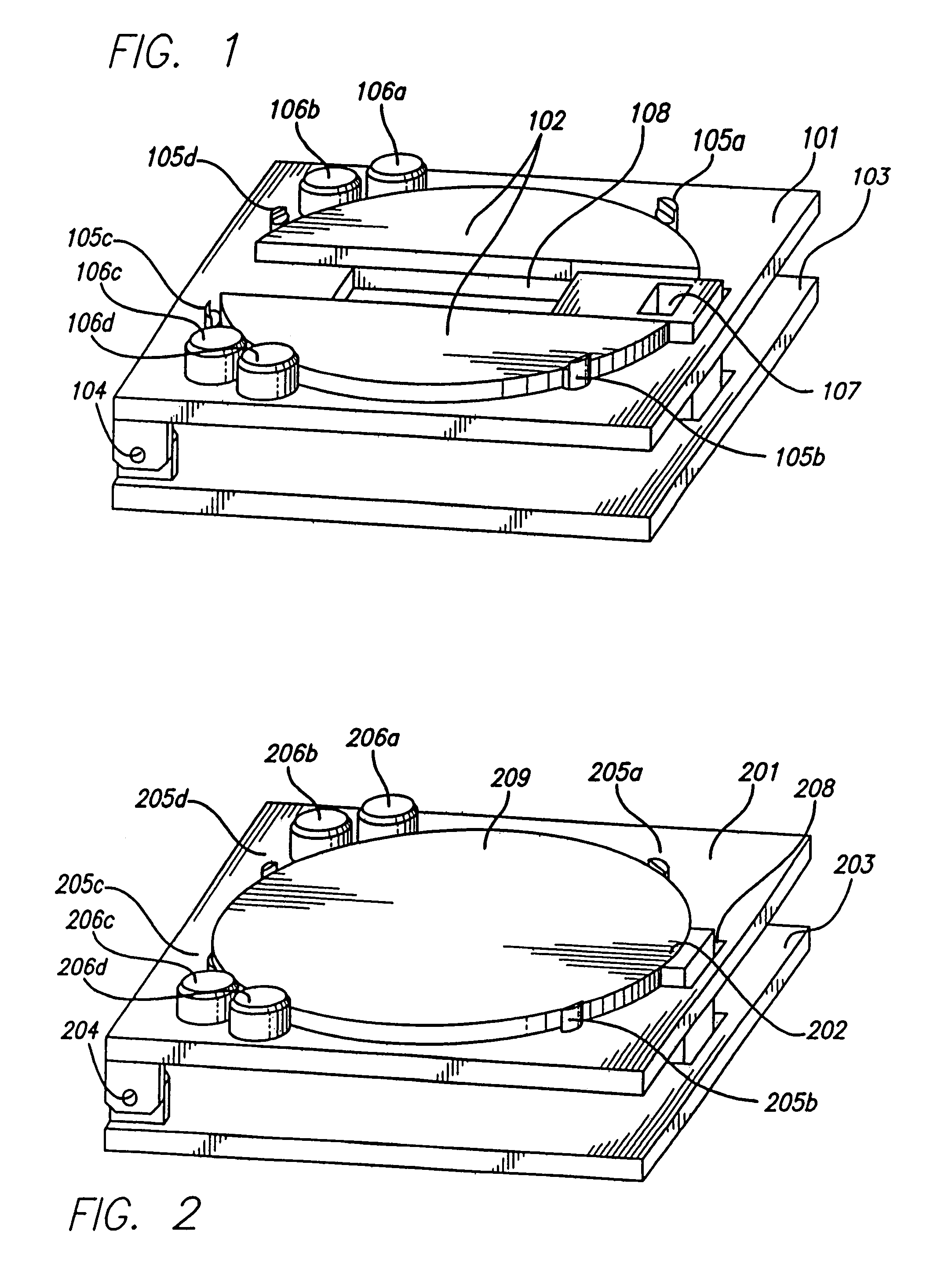
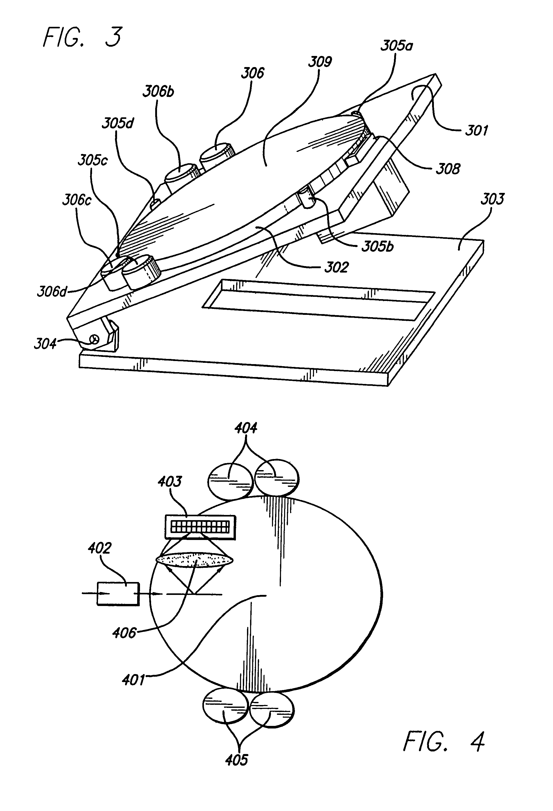
[0029]FIGS. 1–3 present various views of the invention in the loaded and unloaded states. From FIG. 1, the background contamination inspection device is initially in its unloaded state, or without a semiconductor wafer located thereon. The semiconductor wafer is supported by a substantially flat table surface 101. The substantially flat table surface 101 is equipped with an air-bearing mechanism 102 upon which the semiconductor wafer may be floatably supported to eliminate contamination of the backside by contact with the table surface 101. The table surface 101 is mounted to a fixed base 103 such that the table surface 101 can tilt about an axis 104 defined at a side edge of the table surface 101. Four wafer load pins 105a–105d are mounted on the table surface 101 such that they can retract and temporarily maintain the wafer. The wafer load pins 105a–d are located in a circular pattern concentric with the air-bearing mechanism 102 and semiconductor wafer which is to be loaded. Furt...


PUM

PropertyMeasurementUnit
angle of tiltaaaaaaaaaa
sizeaaaaaaaaaa
optical inspectionaaaaaaaaaa

Abstract

A system for simultaneously inspecting the frontsides and backsides of semiconductor wafers for defects is disclosed. The system rotates the semiconductor wafer while the frontside and backside surfaces are generally simultaneously optically scanned for defects. Rotation is induced by providing contact between the beveled edges of the semiconductor wafer and roller bearings rotationally driven by a motor. The wafer is supported in a tilted or semi-upright orientation such that support is provided by gravity. This tilted supporting orientation permits both the frontside and the backside of the wafer to be viewed simultaneously by a frontside inspection device and a backside inspection device.

Description

[0001]This application is a continuation of U.S. patent application Ser. No. 09 / 714,042, filed Nov. 16, 2000, now U.S. Pat. No. 6,559,938, which is a continuation of U.S. Patent Application Ser. No. 09 / 299,698, filed Apr. 26, 1999, now U.S. Pat. No. 6,204,917, which claims the benefit of the filing date of U.S. Provisional Patent Application No. 60 / 101,400, filed Sep. 22, 1998, all of which are hereby incorporated by reference.BACKGROUND OF THE INVENTION[0002]1. Field of the Invention[0003]The present invention relates generally to contamination inspection for semiconductor wafers and the like and in particular to a system which inspects both the frontside and backside of a semiconductor wafer without manual or automatic inversion of the wafer.[0004]2. Description of the Related Art[0005]Tools used in the semiconductor wafer manufacturing process must periodically be checked to determine whether they must be replaced or are still in usable condition. The condition of a tool is check...

Claims


Application Information

Patent Timeline
Patent Type & Authority Patents(United States)
IPC IPC(8): G01N21/88G01N21/95
CPCH01L21/67288G01N21/9501G01N21/94G01N21/9503
Inventor SMEDT, RODNEY G
Owner KLA CORP
Why Eureka
Try Eureka