Electromagnetic apparatus drive apparatus

a technology of electromagnetic devices and drive units, which is applied in the direction of electrical devices, electric motors with armatures, magnetic bodies, etc., can solve problems such as the sound of electromagnetic devices

Inactive Publication Date: 2006-05-09
FUJI ELECTRIC FA COMPONENTS & SYST CO LTD
View PDF12 Cites 7 Cited by
  • Summary
  • Abstract
  • Description
  • Claims
  • Application Information

AI Technical Summary

Benefits of technology

[0034]An object of the present invention is to provide a drive unit for an electromagnetic device capable of reliably releasing an electromagnetic device with a non-conductive interval t1. It is possible to reduce power consumption through constant current control conducted with PWM control of a magnetizing coil current of the electromagnetic device, and also to reduce beat noise of the electromagnetic device in a holding state.

Problems solved by technology

As a result, the attraction force of the electromagnetic device is greatly fluctuated, thereby causing beat sound from the electromagnetic device.

Method used


Image

  • Electromagnetic apparatus drive apparatus
  • Electromagnetic apparatus drive apparatus
  • Electromagnetic apparatus drive apparatus

Examples


first embodiment

[First Embodiment]

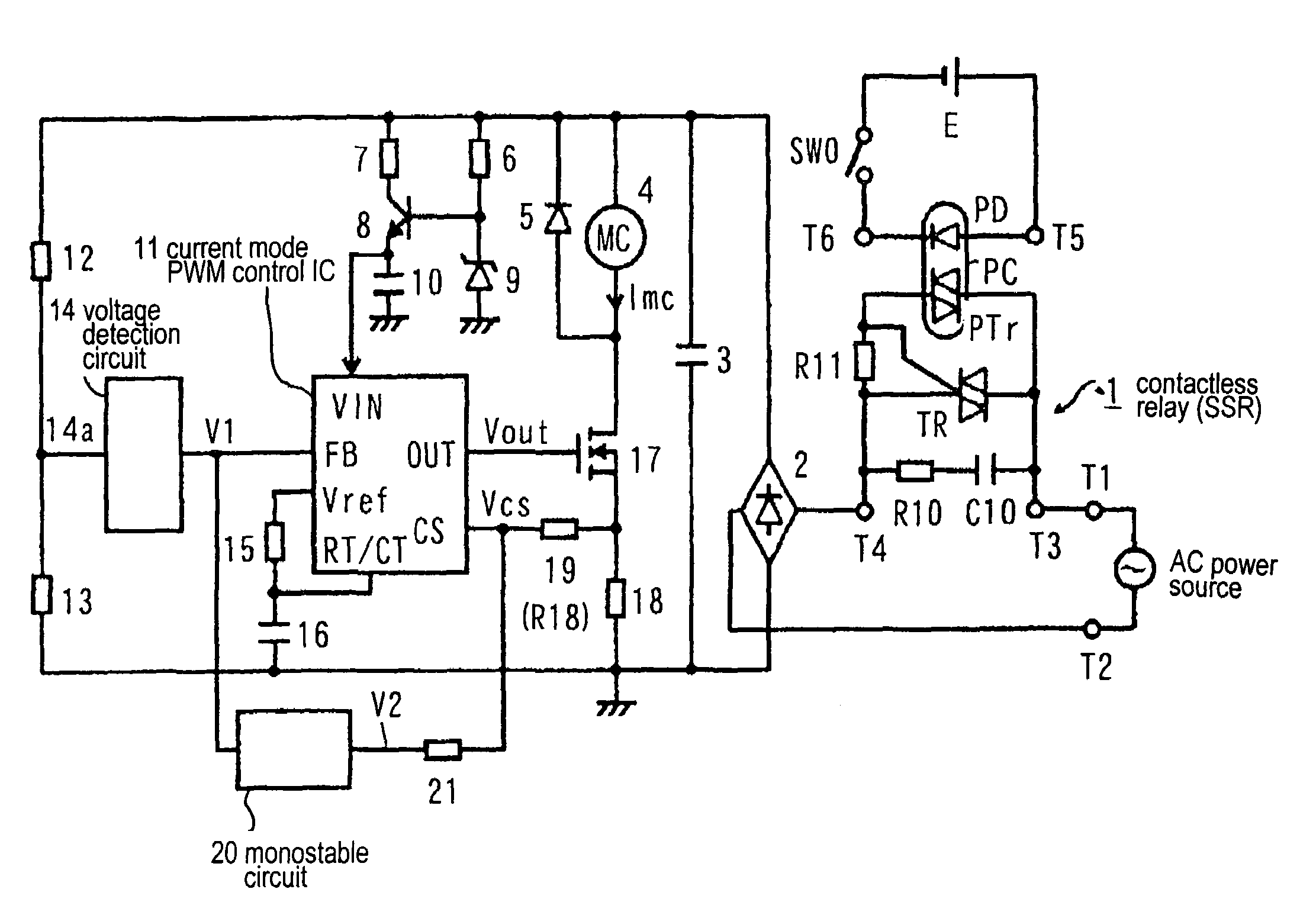
[0052]FIG. 1 shows a circuit diagram of a drive device for an electromagnetic device according to a first embodiment of the present invention. FIG. 6 shows an operational waveform of a main part of the circuit shown in FIG. 1 when the electromagnetic device becomes a hold state. Here, FIG. 1 corresponds to FIG. 4, and FIG. 6 corresponds to FIG. 9.

[0053]The circuit diagram shown in FIG. 1, in addition to the components shown in FIG. 4, comprises a mono-stable circuit 20 and a resistor 21 connected between an output terminal of the mono-stable circuit 20 and a current detection terminal CS of a current mode PWM control IC 11. As shown in FIG. 6, the mono-stable circuit 20 is triggered when a voltage V1 of an H level outputted by a voltage detection circuit 14 decreases within a non-conductive interval t1 centered around a 0 cross point with the AC power source voltage. A voltage V2 of the H level is outputted within a period t2 comprising a plurality of periods T of ...

second embodiment

[Second Embodiment]

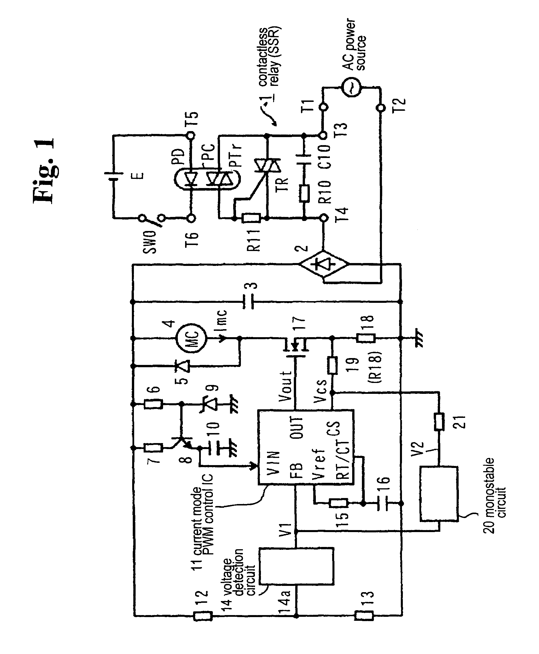
[0057]FIG. 2 shows a circuit diagram of a drive device for an electromagnetic device according to a second embodiment of the present invention. FIG. 7 shows an operational waveform of a main part of the circuit shown in FIG. 2 when the electromagnetic device becomes a hold state. Here, FIG. 2 corresponds to FIG. 4, and FIG. 7 corresponds to FIG. 9.

[0058]The circuit diagram shown in FIG. 2, in addition to the components shown in FIG. 4, comprises a resistor 22 connected between the PWM pulse output terminal OUT of the current mode PWM control IC 11 and the current detection terminal CS. In the circuit shown in FIG. 2, each time the PWM pulse Vout of the H level is outputted, the voltage of the PWM pulse Vout is divided by the resistors 22 and 19 and current detection resistor 18. Accordingly, in this case, the superimposed voltage of the divided voltage component of the PWM pulse Vout, i.e. the voltage applied to the resistor 19, and the voltage (Imc×R18) of the cu...

third embodiment

[Third Embodiment]

[0060]FIG. 3 shows a circuit diagram of a drive device for an electromagnetic device according to a third embodiment of the present invention. FIG. 8 shows an operational waveform of a main part of the circuit diagram shown in FIG. 3 when the electromagnetic device becomes a hold state. Here, FIG. 3 corresponds to FIG. 1, and FIG. 8 corresponds to FIG. 6.

[0061]In the circuit diagram shown in FIG. 3, in addition to the components shown in FIG. 1, an AND circuit 23 having one input terminal connected to the output of the mono-stable circuit 20 is inserted between the mono-stable circuit 20 and the resistor 21, and the other input terminal of the AND circuit 23 is connected to the PWM pulse output terminal OUT of the current mode PWM control IC 11. In the circuit diagram shown in FIG. 3, as shown in FIG. 8, within the interval t2 in which the output V2 of the mono-stable circuit 20 becomes the H level, the interval following the non-conductive interval t1, i.e. the ou...


PUM

PropertyMeasurementUnit
voltageaaaaaaaaaa
voltage Vrefaaaaaaaaaa
voltageaaaaaaaaaa

Abstract

Conventionally, a non-conductive period is provided in a region in the vicinity of zero of an AC power voltage via a voltage detection circuit 14 to turn off reliably. The FET 17 maintains the ON state within several switching cycles after the non-conductive interval to rapidly restore the magnetizing coil current, so that the magnetizing coil current rapidly increases. An object is to suppress beat noise in the electromagnetic device. Within a prescribed interval following the non-conductive interval, a partial voltage at a resistor 19 of an output V2 of a mono-stable circuit 20 is added as a bias voltage to a detection voltage of a magnetizing coil current at a resistor 18, and is detected by the IC 11. The IC 11 drives a FET 17 with a constant switching period after the non-conductive interval, thereby preventing the increase in the magnetizing coil current and resolving the problem.

Description

TECHNICAL FIELD[0001]The present invention relates to a drive unit for an electromagnetic device, in which a drive current for energizing a magnetizing coil of an electromagnetic device is controlled with constant-current control through switching means for switching power source to reduce power consumption of the electromagnetic device. In particular, the present invention relates to a drive unit for an electromagnetic device in which noise generated from the electromagnetic device due to an operation of the switching means is reduced.BACKGROUND OF THE INVENTION[0002]Switching means switches an electric current supplied to a magnetizing coil of an electromagnetic device to reduce power consumption of the electromagnetic device as disclosed in Japanese Patent No. 2626147. In the disclosed technology, a switching control circuit drives power distribution to a magnetizing coil of an electromagnetic device according to an intermittent pulse signal. A main switching element of a contact...

Claims


Application Information

Patent Timeline
Patent Type & Authority Patents(United States)
IPC IPC(8): H01H47/00H01F7/18H01H47/32H02M7/12
CPCH01F7/18H01F7/1844H01H47/325H01F2007/1894H01F2007/1888
Inventor UEKI, KOICHIISHIKAWA, KIMITADA
Owner FUJI ELECTRIC FA COMPONENTS & SYST CO LTD
Why Eureka
Try Eureka