Parallel compression test circuit of memory device

a memory device and compression test technology, applied in information storage, static storage, digital storage, etc., can solve the problems of increasing current consumption, generating noise, and high peak current and noise, and achieve the effect of reducing nois

Inactive Publication Date: 2006-05-16
INTELLECTUAL DISCOVERY CO LTD
View PDF9 Cites 17 Cited by
  • Summary
  • Abstract
  • Description
  • Claims
  • Application Information

AI Technical Summary

Benefits of technology

[0023]Accordingly, it is an object of the present invention to disperse peak cu...

Problems solved by technology

As a result, high peak current and noise can be generated because the write drivers 22 of the four banks 12 are simultaneously operated in the parallel test mode rather than in the normal mode.
Although the example where th...

Method used


Image

  • Parallel compression test circuit of memory device
  • Parallel compression test circuit of memory device
  • Parallel compression test circuit of memory device

Examples


Embodiment Construction

[0033]The present invention will be described in detail with reference to the accompanying drawings.

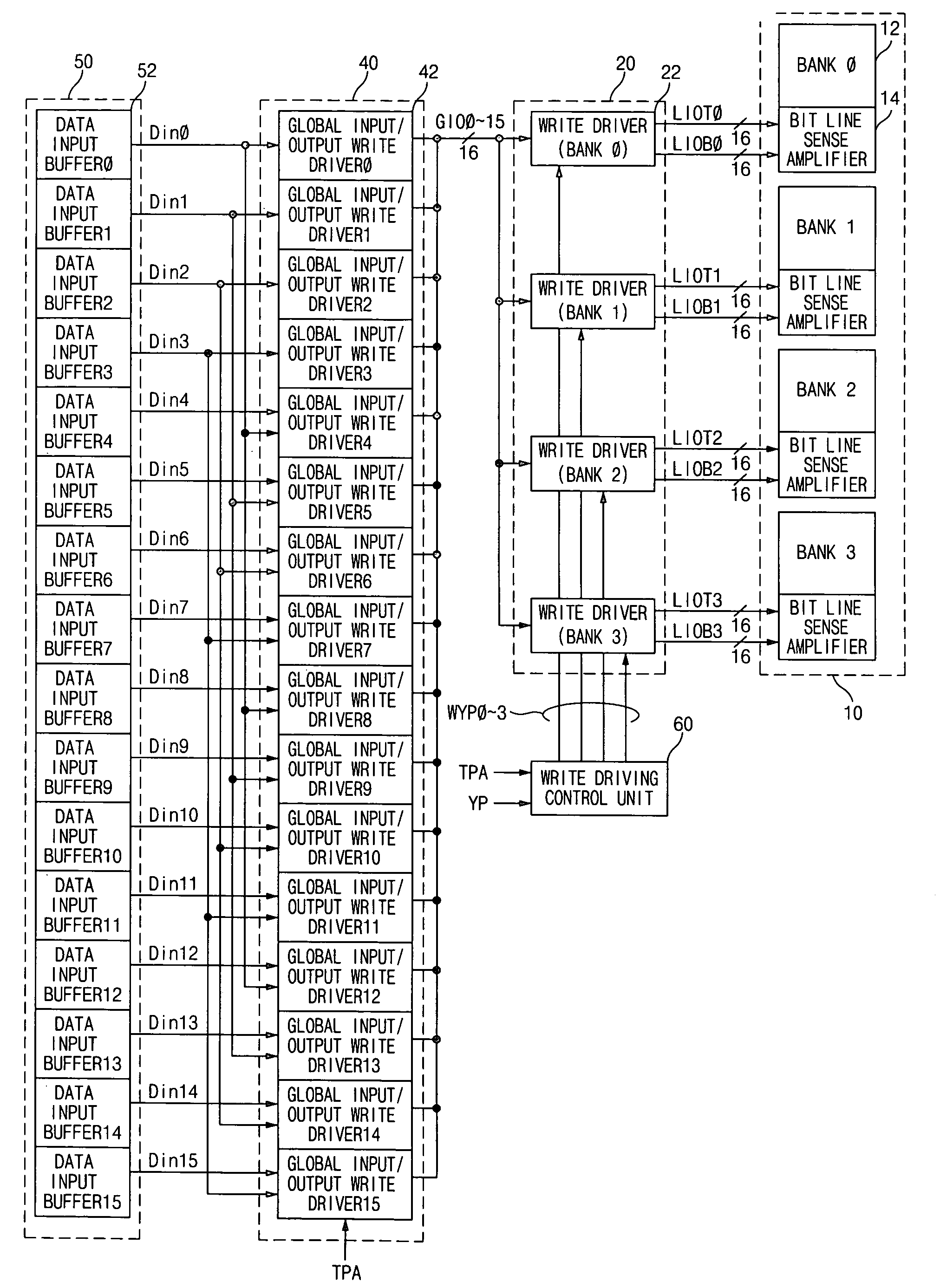
[0034]FIG. 4 is a block diagram illustrating a parallel compression test circuit of a memory device according to an embodiment of the present invention.

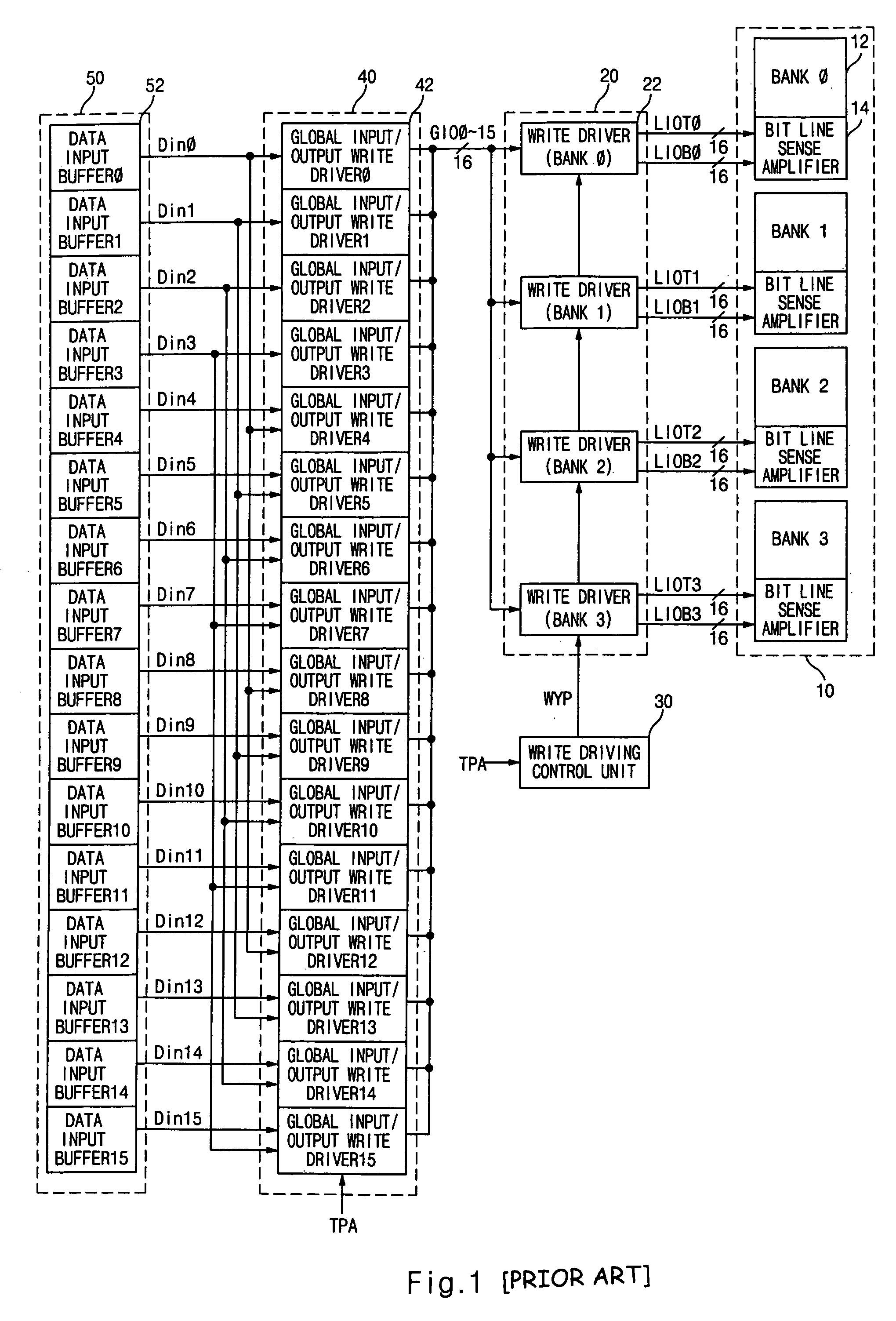
[0035]In the embodiment, the parallel compression test circuit comprises a memory unit 10, a write driving unit 20, a write driving control unit 60, a global input / output write driving unit 40, and a data input buffer 50.

[0036]The memory unit 10 comprises four banks 12 and four bit line sense amplifiers 14. Here, data on local input / output buses LIOT0˜LIOT3 and LIOB0˜LIOB3 are stored in the banks 12 through the bit line sense amplifiers 14.

[0037]The write driving unit 20 comprises four write drivers 22 corresponding to each bank 12. Each write driver 22 drives data on corresponding one of global input / output lines GIO0˜GI015 to transmit the data to the bit line sense amplifiers 14 of the corresponding bank 12.

[0038]The write driving co...


PUM


Abstract

A parallel compression test circuit of a memory device operates write drivers sequentially in a parallel compression test to disperse peak current and reduce noise. The circuit comprises a write driving control unit for generating a plurality of write driving control signals in response to a column operation pulse signal at the same timing in a normal mode, at a different timing in the parallel compression test mode.

Description

BACKGROUND OF THE INVENTION[0001]1. Field of the Invention[0002]The present invention generally relates to a parallel compression test circuit of a memory device, and more specifically, to a technology of sequentially operating write drivers in a parallel compression test mode to disperse current and reduce noise.[0003]2. Description of the Related Art[0004]FIG. 1 is a block diagram illustrating a conventional parallel compression test circuit of a memory device.[0005]The conventional parallel compression test circuit comprises a memory unit 10, a write driving unit 20, a write driving control unit 30, a global input / output write driving unit 40 and a data input buffer 50.[0006]The memory unit 10 comprises four banks 12 and four bit line sense amplifiers 14. Here, data on local input / output buses LIOT0˜LIOT3 and LIOB0˜LIOB3 are stored in the banks 12 through the bit line sense amplifiers 14.[0007]The write driving unit 20 comprises four write drivers 22 corresponding to each bank 12...

Claims


Application Information

Patent Timeline
IPC IPC(8): G11C29/00
CPCG11C29/40G11C2029/2602G11C2029/1202G11C29/00
Inventor KIM, TAEK SEUNG
Owner INTELLECTUAL DISCOVERY CO LTD
Why Eureka
Try Eureka