Optical waveguide transmitter-receiver module

a technology of optical waveguide and transmitter, which is applied in the direction of optical waveguide light guide, instruments, optics, etc., can solve the problems of complex manufacturing process, limited quantity of manufactured units per unit wafer, and complex manufacturing process, so as to reduce the dimensions of the substrate on which light emitting elements and photo-receiving elements are mounted, increase the number of units manufactured from a wafer or similar, and reduce the adhesive area between substrates

Inactive Publication Date: 2006-05-16
NEOPHOTONICS CORP
View PDF9 Cites 8 Cited by
  • Summary
  • Abstract
  • Description
  • Claims
  • Application Information

AI Technical Summary

Benefits of technology

[0024]One object of this invention is to provide an optical waveguide transmitter-receiver module which, by reducing electrical crosstalk, can be made smaller and can be mass-produced.
[0025]A second object of this invention is to provide an optical waveguide transmitter-receiver module which, by decreasing the bonding area with the substrate, reduces the occurrence of malfunctions.
[0026]A third object of this invention is to provide an optical waveguide transmitter-receiver module comprising a mechanism to prevent influx of the adhesive used for improved manufacturing yields.
[0031]By means of a module of this invention, in the case of specifications in which both a light emitting element and a photo-receiving element operate simultaneously, by separating the substrate on which the light emitting element is mounted and the substrate on which the photo-receiving element is mounted, electrical crosstalk between the light emitting element and the photo-receiving element can be simply and appropriately reduced. By this means, the dimensions of substrates on which light emitting element and photo-receiving elements are mounted can be decreased, and the number of units manufactured from a wafer or similar can be increased. Further, in this configuration parts of a first and second substrate are fixed to parts of a third substrate, so that the adhesive areas between substrates can be decreased; consequently, warping of each substrate, strain arising from differences in linear expansion coefficients, stress concentration, and degradation of bonding strength can be reduced.
[0032]In a preferred embodiment of this invention, dicing is used to form dicing grooves in the first and second groove sides, opposing the end of the third groove, the emitting part of the light emitting element and receiving part of the photo-receiving element, respectively. By this means, when for example using adhesive to bond the first, second, and third substrates, excess adhesive resin flows into the dicing grooves, and so prevents flow toward the light emitting element and photo-receiving element.

Problems solved by technology

Conventional silicon platform structures, in which optical waveguides and silicon substrates are united, have problems which include complexity of manufacturing processes and limitations on the manufactured quantity per unit wafer.
Consequently the manufacturing process is complex, and moreover each optical waveguide transmitter-receiver module area formed on the wafer must be made slightly larger in order to expedite manufacturing processes.
Hence such problems as limits on the quantity manufactured per unit wafer arise.
However, if such high-temperature annealing is performed, defects occur in the silicon crystal of the silicon substrate 1, so that highly precise formation of the V groove by etching is made difficult, and consequently the realization of a receptacle structure (an optical connector structure having a function for optical fiber attachment and removal) becomes difficult.
Further, it is structurally difficult to insert the wavelength-selection filter 4 into the PLC substrate 9, and so there is the added problem that versatility of support for STM and ATM is lacking.

Method used


Image

  • Optical waveguide transmitter-receiver module
  • Optical waveguide transmitter-receiver module
  • Optical waveguide transmitter-receiver module

Examples


first embodiment

[0051

[0052]FIG. 4 is a perspective, exploded view of the optical waveguide transmitter-receiver module of a first embodiment of this invention, applicable to a π-PON system.

[0053]In this optical waveguide transmitter-receiver module, a strip or rectangle solid-shaped first substrate (for example, a silicon substrate) 10, on which are mounted optical elements, a strip or rectangle solid-shaped second substrate (for example, a silicon substrate) 20 having the same thickness as the silicon substrate 10, and for connection of optical fibers; and a strip or rectangle solid-shaped third substrate (for example, a PLC substrate) 30, on which is formed an optical waveguide, are separated. These three substrates 10, 20, and 30 are hybrid-integrated in a planar-mounted structure.

[0054]One of the principal surfaces of the silicon substrate 10, which is the upper face (hereafter simply “surface”), is flat, and in this surface, the first groove is formed (for example, an etched groove 11 is forme...

second embodiment

[0063

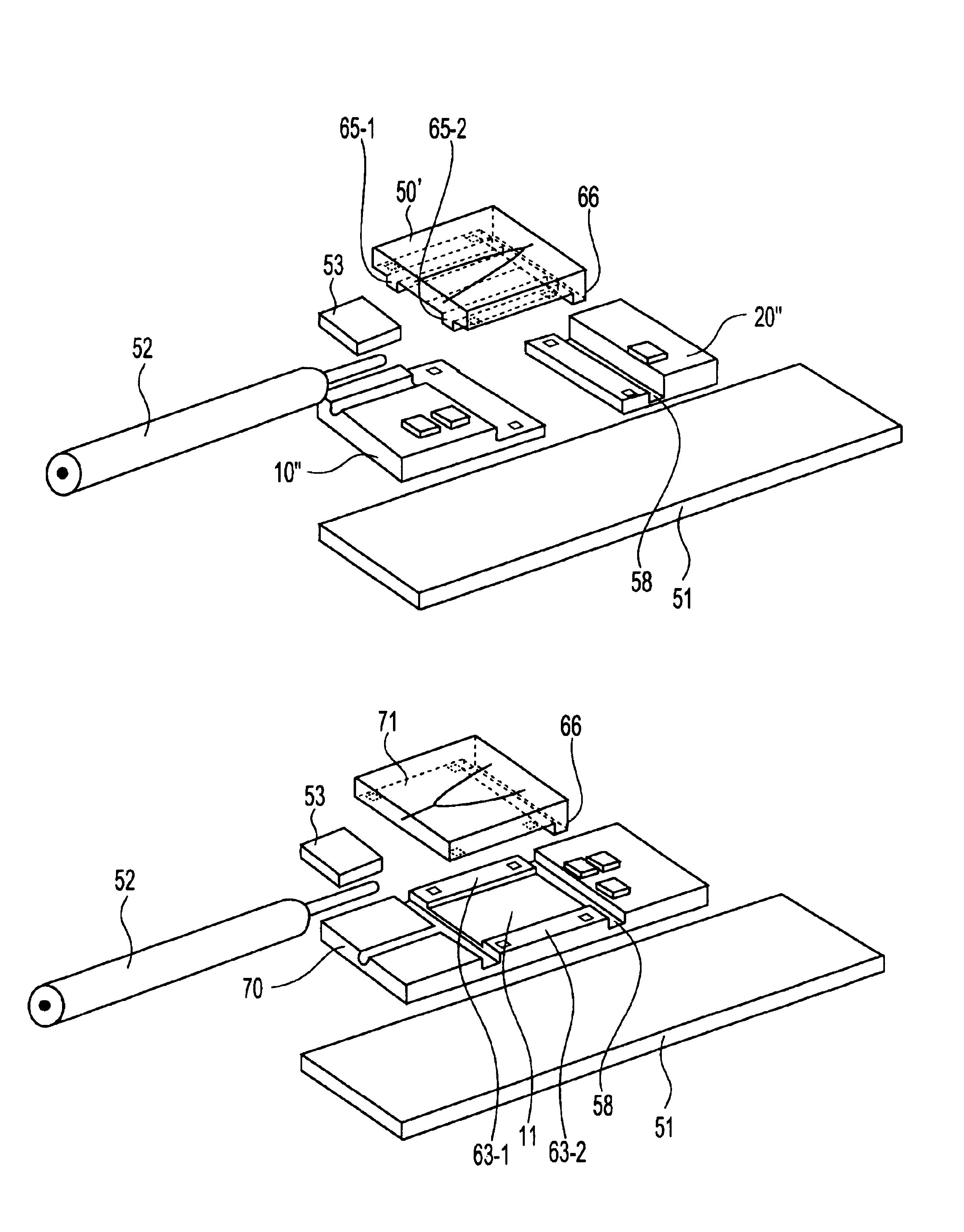
[0064]FIG. 5 is a perspective, exploded view of the optical waveguide transmitter-receiver module of a second embodiment of this invention as an example of application to an STM-PON system. Components which are common with components in FIG. 4, showing the first embodiment, are assigned common symbols.

[0065]In the optical waveguide transmitter-receiver module of the second embodiment, in addition to the V groove 22, another V groove 23 is simultaneously formed by etching in the silicon substrate 20 of FIG. 4. In this configuration example, the V grooves 22 and 23 are formed in parallel; but this does not limit the scope of this invention. The optical waveguide 31A formed in the PLC substrate 30 has entry / exit end faces 31a to 31d; a groove is cut, for example by dicing, in the branching part 31e joining the end faces, and a wavelength-selecting filter 32 is embedded. Otherwise the configuration is similar to that of FIG. 4.

[0066]In the method of manufacture of this optical wave...

third embodiment

[0070

[0071]FIG. 6 is a perspective, exploded view of the optical waveguide transmitter-receiver module of a third embodiment of this invention, as an example of application to an ATM-PON system. Components which are common with components in FIG. 4 and FIG. 5, showing the first and second embodiments, are assigned common symbols.

[0072]For example, in the optical waveguide transmitter-receiver module used in an ATM-PON system, the light emitting element 18 and photo-receiving element 19 operate simultaneously, and electrical crosstalk occurs via the silicon substrate between these elements, exerting adverse effects. Hence of the two separate first and second silicon substrates 10, 20, the photo-receiving element 19 is fixed in place by soldering or other means to the surface of the silicon substrate 10, and the light emitting element 18 is fixed in place by soldering or other means to the surface of the other silicon substrate 20.

[0073]Simultaneously with formation of the V groove 22...


PUM


Abstract

A planar-mounted optical waveguide transmitter-receiver module has a plurality of separated silicon substrates and a PLC substrate hybrid-integrated. In this module, electrical crosstalk between the light emitting element side and photo-receiving element side is reduced, and an adhesion area between substrates is decreased. In this module, a first silicon substrate, on which are mounted a light emitting element and photo-receiving element, is positioned opposing a second silicon substrate, in which is formed a V groove, in which an optical fiber is to be inserted and fixed in place with resin or by other means. On joining surfaces of the first silicon substrate and joining surfaces of the second silicon substrate are positioned and fixed in place joining surfaces on the back face of the optical waveguide (PLC) substrate, in which is formed an optical waveguide. By this means, the light emitting element, the photo-receiving element, and the optical fiber inserted into the V groove are optically aligned with and simultaneously optically coupled with the optical waveguide of the PLC substrate.

Description

[0001]This is a Continuation-In-Part of parent application Ser. No. 09 / 818,894, filed Mar. 28, 2001, now U.S. Pat. No. 6,456,767.BACKGROUND OF THE INVENTION[0002]1. Field of the Invention[0003]This invention concerns a planar-mounted optical waveguide transmitter-receiver module, in which silicon or other substrates, separated into a plurality of substrates, and an optical waveguide (planar lightwave circuit) substrate (hereafter “PLC substrate”), are hybrid-integrated.[0004]2. Description of Related Art[0005]Optical terminal devices for use in optical subscriber systems are subjected to such demands as smaller integration sizes, multi-functionality, and reduced prices. Optical modules with optical waveguides as devices effective for satisfying such demands are coming into widespread use. Conventional silicon platform structures, in which optical waveguides and silicon substrates are united, have problems which include complexity of manufacturing processes and limitations on the man...

Claims


Application Information

Patent Timeline
Patent Type & Authority Patents(United States)
IPC IPC(8): G02B6/12G02B6/30G02B6/42
CPCG02B6/42G02B6/4246G02B6/30G02B6/423G02B6/4224G02B6/4243G02B6/4245G02B6/4215
Inventor TERASHIMA, TOKIHIRO
Owner NEOPHOTONICS CORP
Why Eureka
Try Eureka