

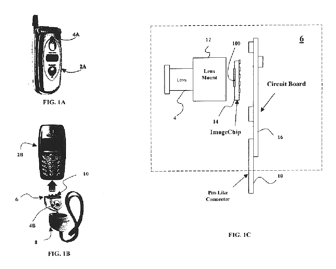
Camera with MOS or CMOS sensor array
a sensor array and camera technology, applied in the field of cameras with mos or cmos sensor arrays, can solve the problems of large energy consumption of small cameras using ccd sensors, inability to use photo-sensing, and problems for today's mobile appliances
- Summary
- Abstract
- Description
- Claims
- Application Information
AI Technical Summary
Benefits of technology
Problems solved by technology
Method used
Image

Examples
Embodiment Construction
In the following description of preferred embodiments, reference is made to the accompanying drawings, which form a part hereof, and which show by way of illustration a specific embodiment of the invention. It is to be understood by those of working skill in this technological field that other embodiments may be utilized, and structural, electrical, as well as procedural changes may be made without departing from the scope of the present invention.
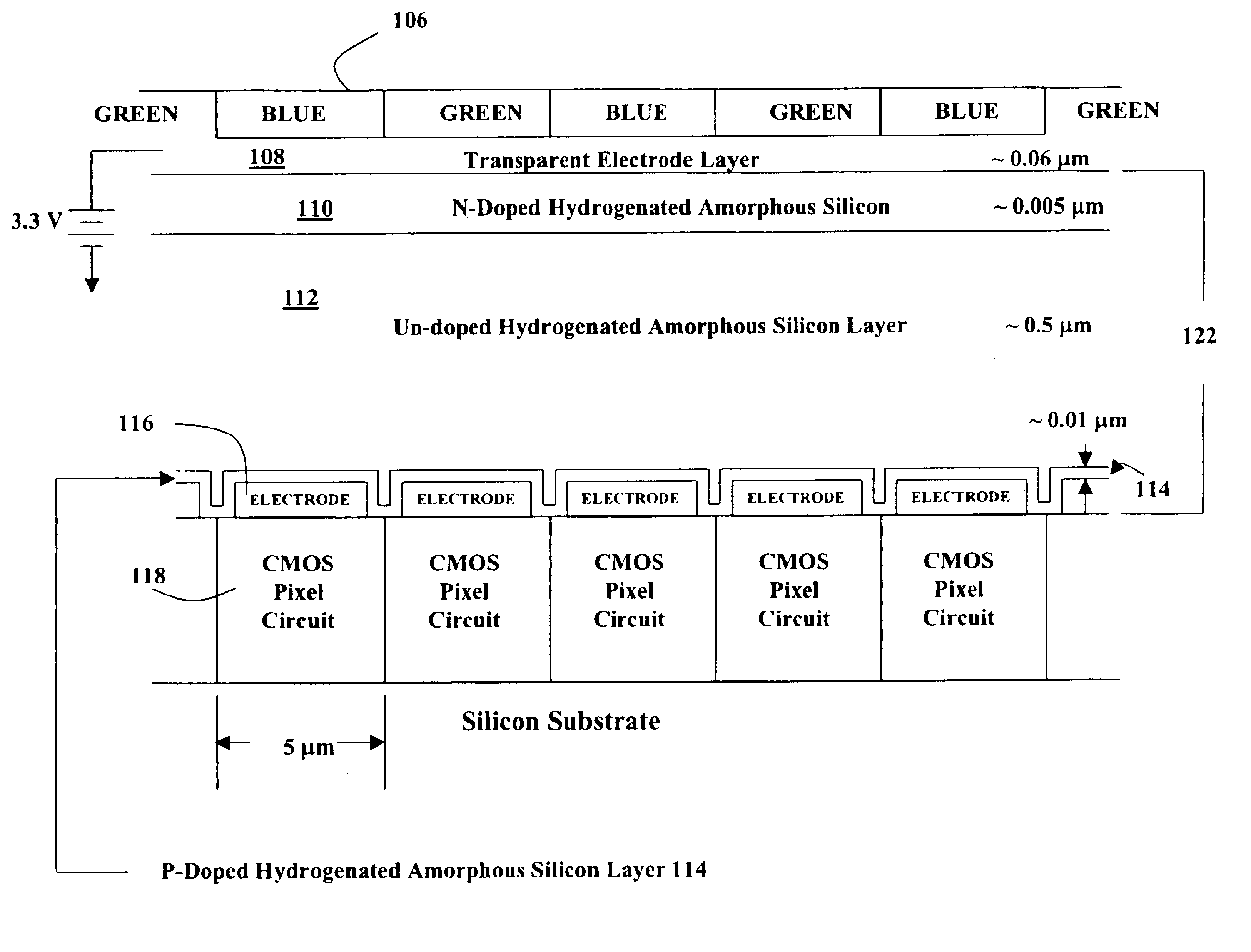
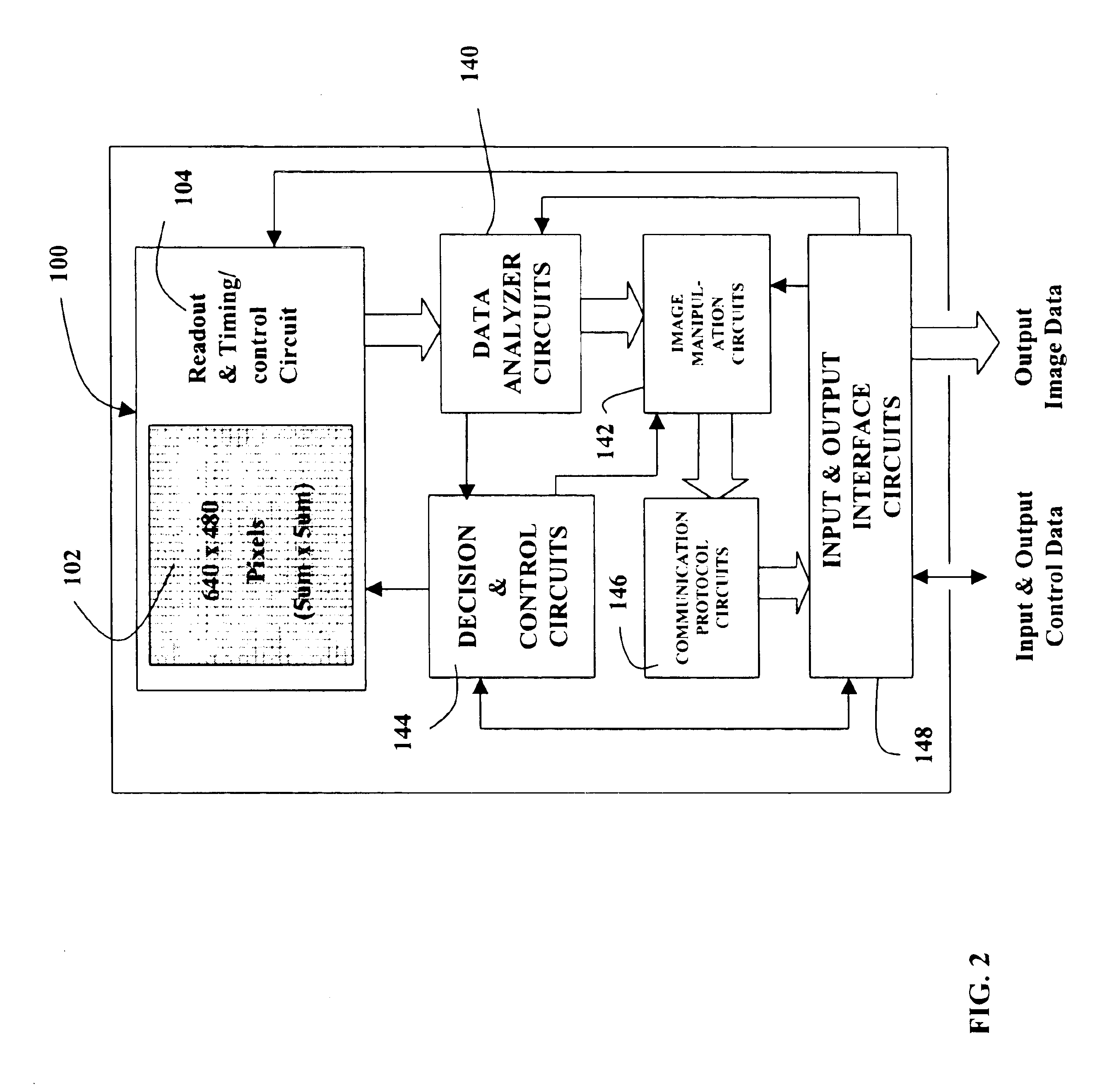
Single Chip Camera with Photo Conductor on Active Pixel Sensor A preferred embodiment of the present invention is a single chip camera with a sensor consisting of a photodiode array consisting of photoconductive layers on top of an active array of CMOS circuits. (Applicants refer to this sensor as a "POAP Sensor" the "POAP" referring to "Photoconductor On Active Pixel".) In this sensor there are 307,200 pixels arranged in as a 640.times.480 pixel array and there is a transparent electrode on top of the photoconductive layers. The pixels ar...
PUM
 Abstract
Description
Claims
Application Information