Pillar cell flash memory technology

a technology of flash memory and pillar cell, which is applied in the direction of solid-state devices, instruments, semiconductor devices, etc., can solve the problems of prohibitive power consumption of sup>2/sup>*f, and achieve the effect of improving programming characteristics

Active Publication Date: 2006-05-23
SANDISK TECH LLC
View PDF24 Cites 102 Cited by
  • Summary
  • Abstract
  • Description
  • Claims
  • Application Information

AI Technical Summary

Benefits of technology

[0008]The present invention provides structures and technique for fabricating a pillar-type nonvolatile memory cell, where each memory cell in an array is isolated from adjacent memory cells by a trench. Each memory cell is formed by a stacking process layers on a substrate: tunnel oxide layer, polysilicon floating gate layer, ONO or oxide layer, polysilicon control gate layer, polysilicon control line layer, another oxide layer, and a polysilicon select gate layer. Many steps of the process are self-aligned. Because of the trench isolations along both the bit line and the word line directions, the disturb effects of performing one operation on one memory cell and having that operation disturb adjacent memory cells is reduced. An array of these memory cells will require fewer segmentations, saving up to fifteen percent in die size as compared to a prior implementation. Furthermore, the memory cell has enhanced programming characteristics because electrons are directed at a nearly normal angle to the floating gate.
[0009]Nearest neighbor capacitive interference is practically eliminated. Tunnel oxide thickness uniformity has enhanced the cycling endurance. Cross point delivery of programming and erase voltages reduces the associated disturb mechanisms. Single cell erase operation is made possible. Single row erase operation is also possible reducing the erase block size. Higher operating word line voltages will reduce virtual ground array current sneak paths. Floating gate channels are vertical and, therefore not subject to decreasing channel lengths as technology is scaled down.
[0010]Note that in a specific embodiment, the ONO layer does not come near the channel. This may help to reduce the effects that charge trap-up (at the oxide-nitride interfaces -and within the nitride layer) may have on memory transistor channel characteristics. Blanket processing may be used all the way to poly-2 deposition. Control gate and control line are in two different layers. Select gate channel may be very long with no area cost. Disturbs are reduced because high voltages are rectangulated to a cell. So some of the burden is carried by the word line and some of it by the control line, and as a result neither will have to go to such extreme voltages as to cause disturbs. Given a targeted cell, cells on the same word line are distinct from cells on the same control line or bit line. Therefore disturb is reduced. High injection efficiency means programming is possible with shorter durations and smaller voltages / currents, and therefore again less disturb. High select-gate VT translates into less disturb. Less disturb, and higher program efficiency means fewer bit line and control line segmentations necessary. Metal word lines (with lower RC time constants), and high coupling of select gate to floating gate means noise can be suppressed by applying AC signals to the word line during read. Since the cells being read are on the same word line, a single AC driven word line will suppress the noise of all the cells in the sector.

Problems solved by technology

So some of the burden is carried by the word line and some of it by the control line, and as a result neither will have to go to such extreme voltages as to cause disturbs.
The associated (½)CV2*f power consumption would have been prohibitive.

Method used


Image

  • Pillar cell flash memory technology
  • Pillar cell flash memory technology
  • Pillar cell flash memory technology

Examples


Embodiment Construction

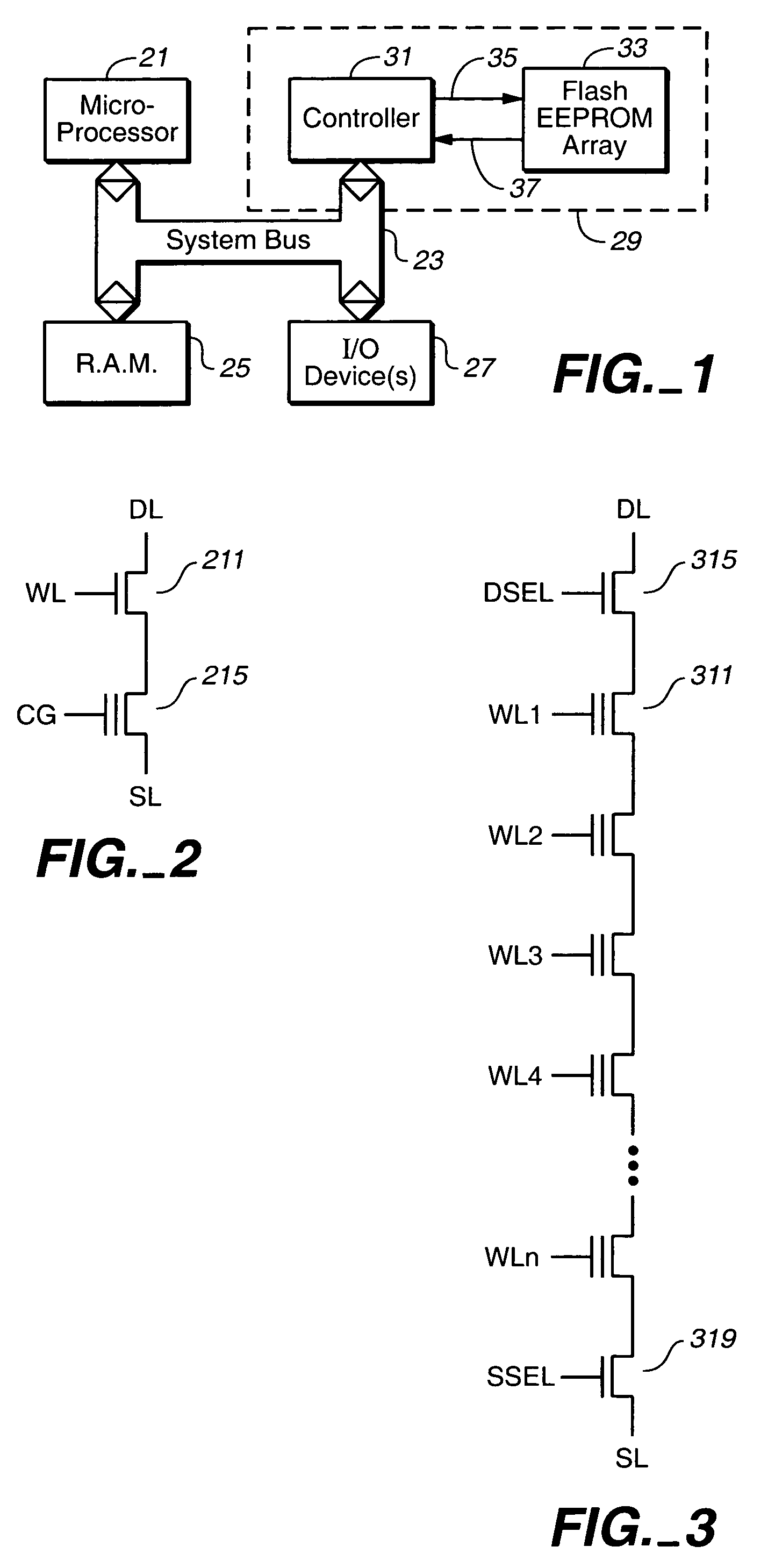
[0046]FIG. 1 generally shows an electronic system, such as a computer system, in which various aspects of the present invention may be incorporated. Some examples of electronics systems include computers, laptop computers, handheld computers, palmtop computers, personal digital assistants (PDA), MP3 and other audio players, digital cameras, video cameras, electronic game machines, wireless and wired telephony devices, answering machines, voice recorders, and network routers.

[0047]This electronic system architecture includes a processor or microprocessor 21 connected to a system bus 23, along with random access, main system memory 25, and at least one or more input-output devices 27, such as a keyboard, monitor, modem, and the like. Another main computer system component that is connected to a typical computer system bus 23 is an amount of long-term, nonvolatile memory 29. In contrast to volatile memory such as DRAM (dynamic RAM) or SRAM (static RAM), nonvolatile memory retains its s...


PUM


Abstract

An array of a pillar-type nonvolatile memory cells (803) has each memory cell isolated from adjacent memory cells by a trench (810). Each memory cell is formed by a stacking process layers on a substrate: tunnel oxide layer (815), polysilicon floating gate layer (819), ONO or oxide layer (822), polysilicon control gate layer (825). Many aspects of the process are self-aligned. An array of these memory cells will require less segmentation. Furthermore, the memory cell has enhanced programming characteristics because electrons are directed at a normal or nearly normal angle (843) to the floating gate (819).

Description

BACKGROUND OF THE INVENTION[0001]The present invention relates to nonvolatile erasable programmable memories and more specifically, structures and fabrication techniques for a pillar structure memory cell storage element.[0002]Memory and storage is one of the key technology areas that is enabling the growth in the information age. With the rapid growth in the Internet, World Wide Web (WWW), wireless phones, personal digital assistants (PDAs), digital cameras, digital camcorders, digital music players, computers, networks, and more, there is continually a need for better memory and storage technology.[0003]A particular type of memory is nonvolatile memory. A nonvolatile memory retains its memory or stored state even when power is removed. Some types of nonvolatile erasable programmable memories include as Flash, EEPROM, EPROM, MRAM, FRAM, ferroelectric, and magnetic memories. Some nonvolatile storage products include CompactFlash (CF) cards, MultiMedia cards (MMC), secure digital (SD...

Claims


Application Information

Patent Timeline
Patent Type & Authority Patents(United States)
IPC IPC(8): H01L29/788G11C16/04H01L21/336H01L21/8247H01L27/115H01L29/423
CPCH01L27/115H01L27/11521H01L29/7883H01L29/42336H01L29/66825H01L29/42328G11C16/0458H10B69/00H10B41/30G11C16/00B82Y10/00
Inventor MOKHLESI, NIMALUTZE, JEFFREY W.
Owner SANDISK TECH LLC
Why Eureka
Try Eureka