Fabrication method of semiconductor device

a technology of semiconductor devices and fabrication methods, which is applied in the direction of semiconductor devices, semiconductor/solid-state device details, electrical devices, etc., can solve the problems of cracking in the semiconductor wafer, the adhesive sticking to the front surface of the semiconductor wafer cannot be completely removed, and the bending strength of the semiconductor wafer may be reduced

Active Publication Date: 2006-05-30
INVENSAS CORP
View PDF13 Cites 24 Cited by
  • Summary
  • Abstract
  • Description
  • Claims
  • Application Information

AI Technical Summary

Benefits of technology

[0025]The present invention was made in view of the foregoing problems, and it is an object of the present invention to provide a fabrication method of a semiconductor device, whereby a reinforcing material is quickly detached from a semiconductor wafer without bending or cracking the semiconductor wafer, when the reinforcing material is used to grind the semiconductor wafer.
[0027]The injection path (hole or groove) of the reinforcing plate connects the interface of the reinforcing plate and the adhesive layer (the interface being a back surface of the reinforcing plate) with a front surface or side surface of the reinforcing plate. The front surface of the semiconductor wafer bears one or more semiconductor devices, and the back surface of the semiconductor wafer is subjected to grinding. The front surface of the semiconductor wafer is bonded with the reinforcing plate via the adhesive layer. The reinforcing plate enables the back surface of the semiconductor wafer to be ground while reinforcing the semiconductor wafer. In this way, a thin semiconductor wafer can be realized without causing cracking or bending.
[0028]In the detaching step, a solvent for dissolving the adhesive layer is injected through the injection path, so that the solvent directly permeates the interface of the reinforcing plate and the adhesive layer. This enables the adhesive layer to be dissolved in a short period of time, thereby quickly eliminating the adhesion force acting between the reinforcing plate and the semiconductor wafer. Thus, with the method for the present invention, the reinforcing plate can be detached from the semiconductor wafer more quickly than with a conventional method in which the adhesive layer is dissolved from the sides.
[0029]Further, because no mechanical stress is exerted on the semiconductor wafer when it is detached, the semiconductor wafer can be detached from the reinforcing plate without causing cracking, chipping, or bending.
[0030]Further, because the method prevents the solvent from touching the dicing tape, the method is also advantageous in, for example, attaching a dicing tape on the back surface of the semiconductor wafer when the dicing tape is used to support the semiconductor wafer when it is separated. Thus, with a fabrication method of the present invention, the detaching step can be carried out without removing the dicing tape.

Problems solved by technology

While the method is pervasive for it offers good productivity, a drawback of the method is that it may produce micro cracks in the back surface of the semiconductor wafer when the semiconductor wafer is ground, with the result that the bending strength of the semiconductor wafer may be reduced.
While the method using a UV curable adhesive can reduce the adhesion force of the adhesive to a certain point by irradiation of UV light, it cannot completely remove the adhesive sticking to the front surface of the semiconductor wafer 33a.
Another drawback of the conventional methods is that the reinforcing plate 31 requires a material that transmits UV light 46.
The methods using a thermoplastic adhesive may also cause the problem of cracking in the semiconductor wafer 33a when the reinforcing plate 31 is detached from the semiconductor wafer 33a.
This makes it extremely difficult to handle the semiconductor wafer 33a without causing cracking or chipping.
However, in this case, the semiconductor wafer 33a may be cracked or bent when the dicing tape is pressed against the back surface of the semiconductor wafer 33a.
This is problematic in that it takes time to completely dissolve the adhesive layer 32 and thereby enables the reinforcing plate 31 to be detached from the semiconductor wafer 33a.
Another drawback is that the adhesive layer 32 is not dissolved uniformly when the adhesive layer 32 is gradually dissolved from the periphery.

Method used


Image

  • Fabrication method of semiconductor device
  • Fabrication method of semiconductor device
  • Fabrication method of semiconductor device

Examples


first embodiment

[0039][First Embodiment]

[0040]Referring to FIGS. 1 (a) through 1(g), and FIG. 2, a First Embodiment of the present invention is described below.

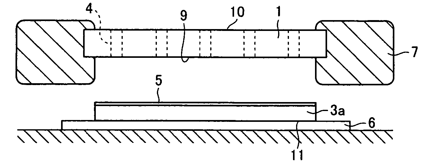
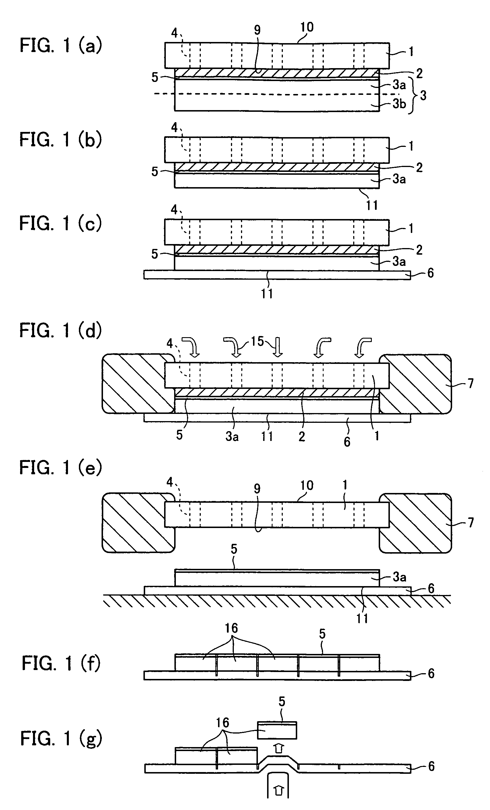
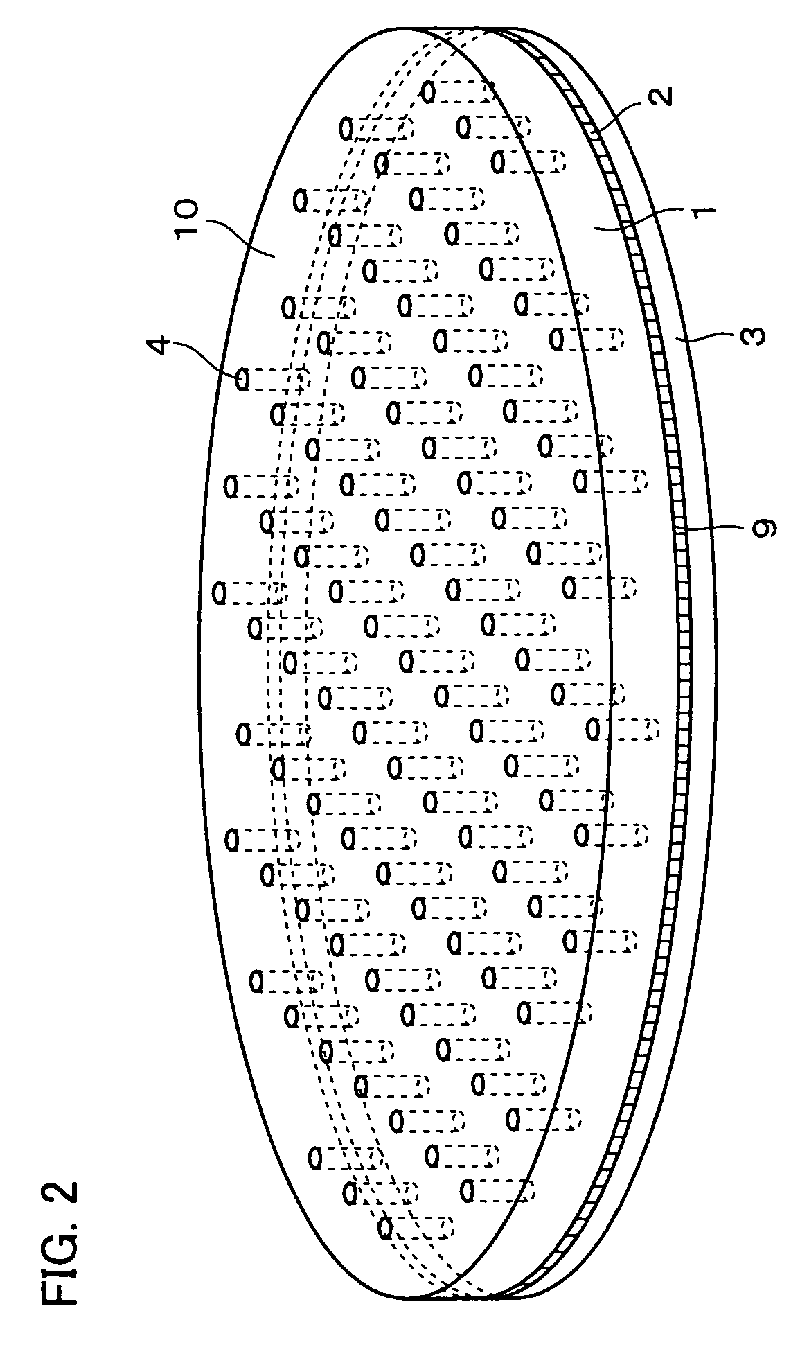
[0041]The present embodiment provides the following five fabrication steps (Step 1 (S1) through Step 5 (S5)). In Step 1, a reinforcing plate 1 and a semiconductor wafer 3 (3a, 3b) are bonded with each other with an adhesive layer 2 interposed in between (reinforcing step, FIG. 1(a)). In Step 2, the semiconductor wafer 3b is ground (grinding step, FIG. 1(b)). In Step 3, a dicing tape 6 is attached on a back surface 11 of the semiconductor wafer 3a (bonding step, FIG. 1(c)). In step 4, a solvent 15 is injected through holes 4 of the reinforcing plate 1, so as tot separate the semiconductor wafer 3a from the reinforcing plate 1 (detaching step, FIGS. 1(d) and 1(e)). In step 5, the semiconductor wafer 3a is diced after it is separated from the reinforcing plate 1, and individual pieces of semiconductor device 16 are picked up (dicing step, FIGS....

second embodiment

[0052][Second Embodiment]

[0053]Referring to FIG. 3(a) through FIG. 3(g), and FIG. 4, a Second Embodiment of the present invention is described below. FIG. 3(a) through FIG. 3(g) illustrate fabrication steps of the present embodiment.

[0054]First, as illustrated in FIG. 3(a), a reinforcing plate 21 and a semiconductor wafer 3 (3a, 3b) are bonded with each other, with an adhesive layer 2 interposed in between (reinforcing step (S1)). A multiplicity of semiconductor devices (not shown) makes up a front surface 5 of the semiconductor wafer 3. The reinforcing plate 21 has a back surface 9 (facing the semiconductor wafer 3 via the adhesive layer 2) with narrow grooves 8, as illustrated in FIG. 4.

[0055]As shown in FIG. 4, the narrow grooves 8 are provided in the form of a lattice throughout the back surface 9 of the reinforcing plate 21. Each narrow groove 8 extends to the side surface of the reinforcing plate 21, and has ends 8a (on the side surface of the reinforcing plate 1) that constit...


PUM


Abstract

A fabrication method of a semiconductor device according to the present invention includes the steps of: bonding a reinforcing plate with a front surface of a semiconductor wafer via a reinforcing plate, the reinforcing plate having holes and the semiconductor wafer bearing semiconductor devices; grinding a back surface of the semiconductor wafer; and detaching the reinforcing plate from the semiconductor wafer by injecting a solvent for dissolving an adhesive layer into the holes and by allowing the solvent to permeate through the adhesive layer. The method enables the reinforcing plate to be quickly detached from the semiconductor wafer without causing defects, such as bending and cracking, in the semiconductor wafer after the reinforcing plate is used to grind the semiconductor wafer.

Description

[0001]This Nonprovisional application claims priority under 35 U.S.C. § 119(a) on patent application Ser. No. 2003 / 089348 filed in Japan on Mar. 27, 2003, the entire contents of which are hereby incorporated by reference.FIELD OF THE INVENTION[0002]The present invention relates to fabrication methods of semiconductor devices, in which, for example, a thin layer of semiconductor wafer is prepared and diced to obtain individual semiconductor devices.BACKGROUND OF THE INVENTION[0003]With a current demand for three-dimensional stacking or high-density packaging of semiconductor devices, it is important nowadays to provide thin semiconductor wafers. One method to provide a thin semiconductor wafer is to lap (grind) the back surface of a semiconductor wafer with a grind stone. While the method is pervasive for it offers good productivity, a drawback of the method is that it may produce micro cracks in the back surface of the semiconductor wafer when the semiconductor wafer is ground, with...

Claims


Application Information

Patent Timeline
Patent Type & Authority Patents(United States)
IPC IPC(8): H01L21/44H01L21/02H01L21/301H01L21/68
CPCH01L21/6835H01L21/6836H01L24/27H01L2221/68327H01L2221/6834H01L2221/68363H01L2221/68381H01L2224/274H01L2924/3512H01L2924/00
Inventor KURIMOTO, HIDEYUKIDOTTA, YOSHIHISAKIMURA, TOSHIO
Owner INVENSAS CORP
Why Eureka
Try Eureka