Increased emission efficiency in organic light-emitting devices on high-index substrates

a light-emitting device and high-index technology, applied in the direction of organic semiconductor devices, discharge tubes/lamp details, discharge tubes luminescnet screens, etc., can solve the problems of light loss due to waveguide and light loss in the ito/organic layer, and achieve the effect of enhancing the light output of the oled

Inactive Publication Date: 2006-05-30
UNIVERSAL DISPLAY +1
View PDF30 Cites 36 Cited by
  • Summary
  • Abstract
  • Description
  • Claims
  • Application Information

AI Technical Summary

Benefits of technology

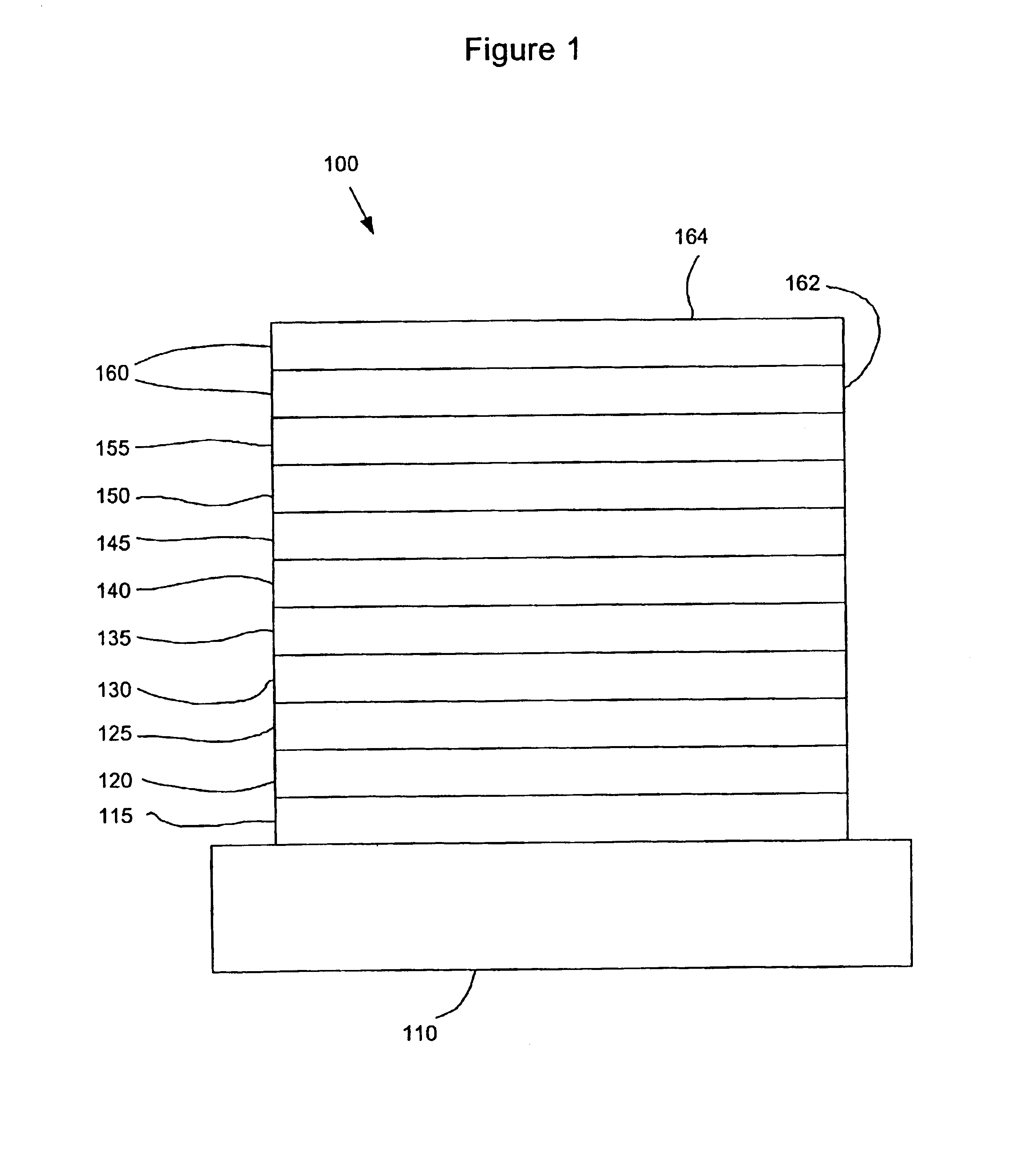
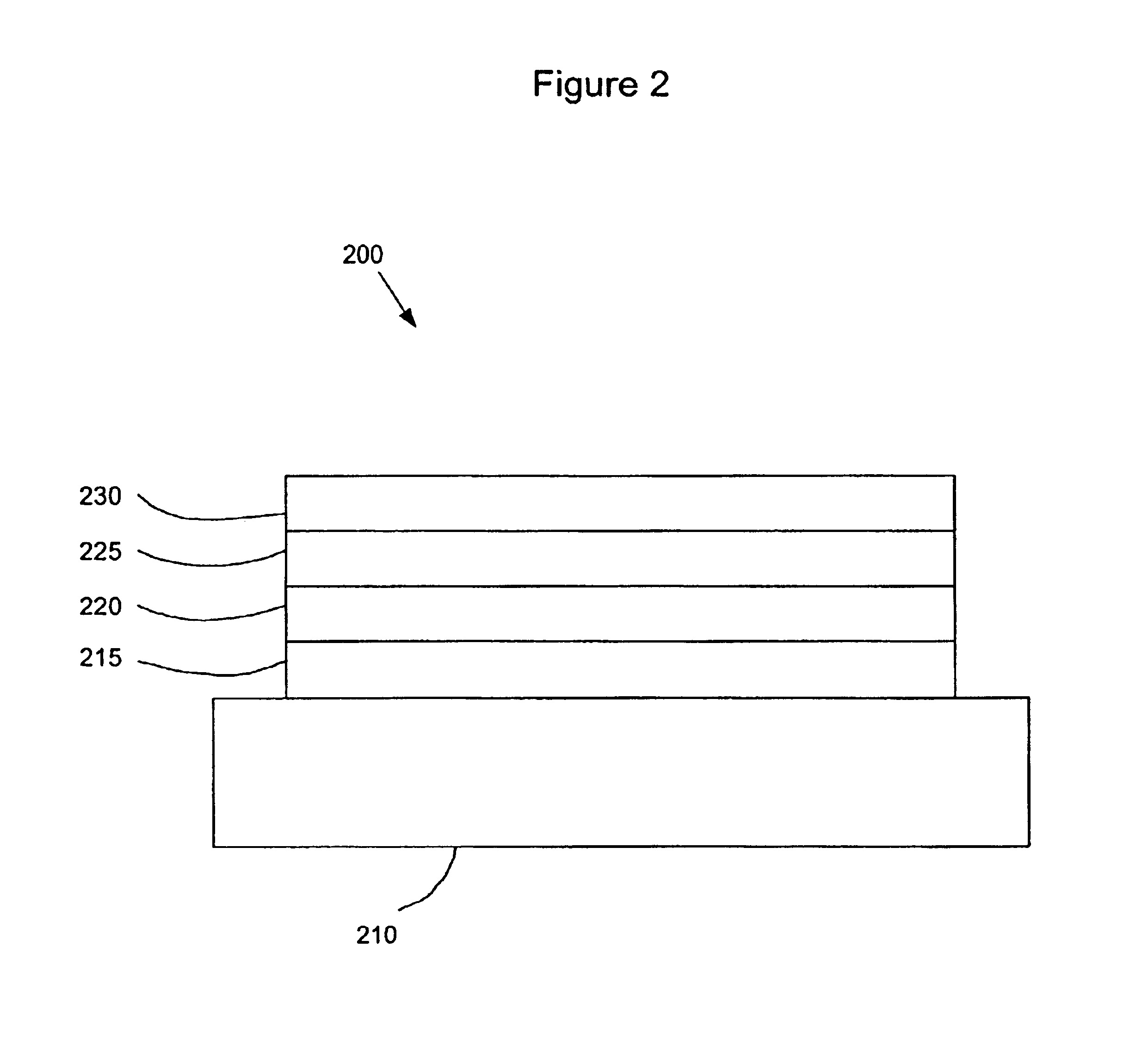
[0013]A device is provided. The device includes a substrate, a first electrode disposed over the substrate, a small molecule organic emissive layer disposed over the first electrode, and a second electrode disposed over the organic emissive layer. The substrate has a first index of refraction, and the organic emissive layer has a second index of refraction. The first index of refraction is higher than the second index of refraction. The device may have an external electroluminescent efficiency of at least about 56%. Bulky substituents or dopants may be used to decrease the index of refraction and / or the density of the organic emissive layer.
[0015]There are at least two advantages in employing shaped high-index substrates. First, in OLEDs on planar substrates, light is lost due to waveguiding in both the substrate and the ITO / organic layer. Shaped standard substrates capture light waveguided in the substrate layer and redirect it externally; however, the light in the ITO / organic layer is still lost. Although the external emission of OLEDs on planar standard and high-index substrates are the same, high-index substrates reduce or eliminate the light waveguided in the ITO / organic layer and leaves more light to be harvested by the shaped substrate. The measured total external emission in the entire forward half space and the forward 120° cone from LEDs on shaped standard substrates are increased by factors of 1.5× and 1.7×, respectively, over devices on planar substrates. With the approach of embodiments of the present invention, the amount of increase becomes 2.3× and 2.9× over OLEDs fabricated on planar substrates—a further improvement of 80% and 120%, respectively, Furthermore, OLEDs fabricated on high-index substrate whose backside is roughened by abrasion shows an increase of 39% in total external emission over an OLED on un-roughened substrates, compared with only a 17% increase for OLEDs on a similarly treated standard glass substrate.
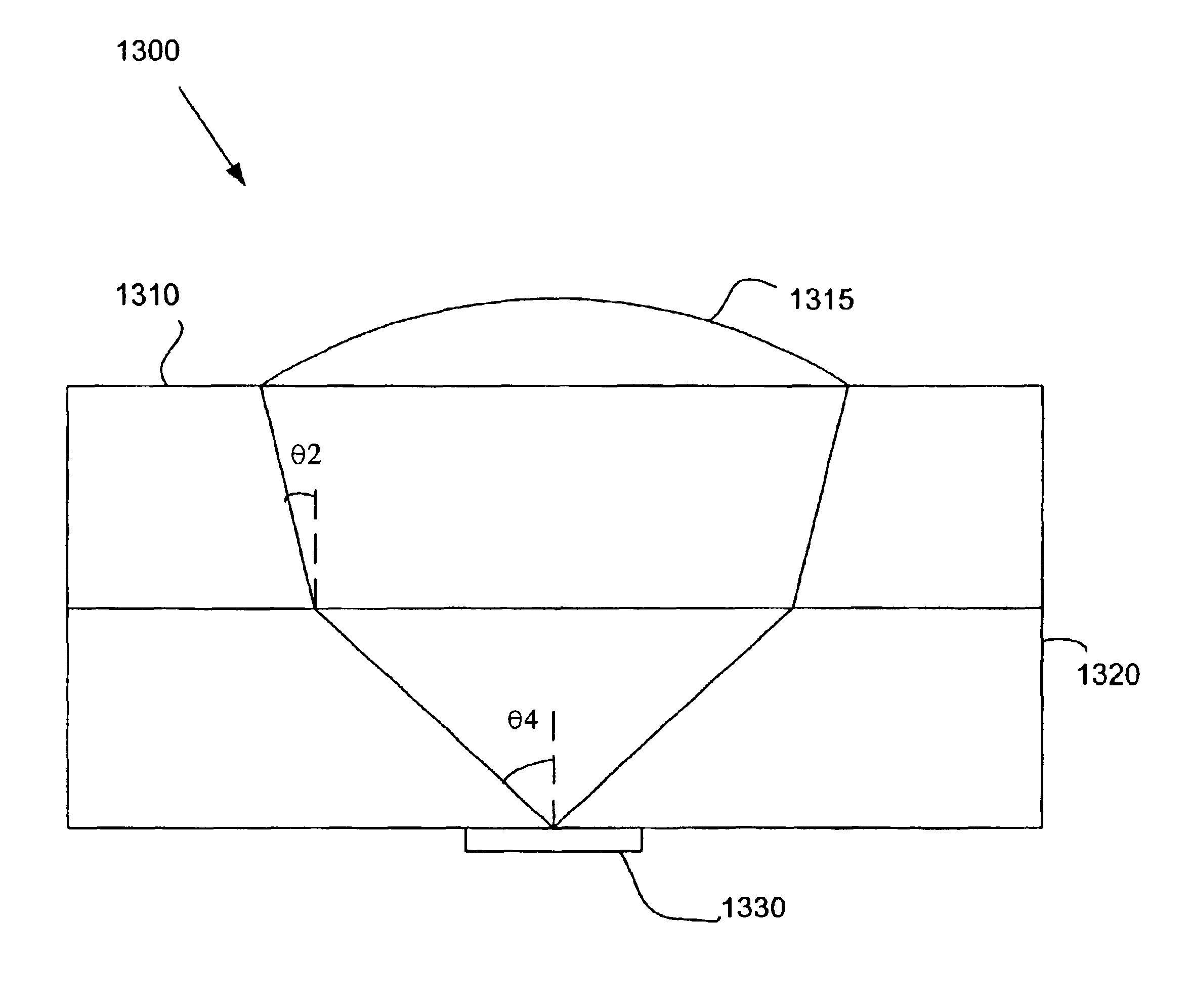
[0016]A second advantage of high-index substrate is that the rays of light in the substrate are refracted towards the normal direction; consequently, a lens on the backside of high-index substrate collects more light compared with a lens of the same size on the backside of a standard substrate. Since the rays of the light collected by the lens are emitted externally, the high-index lens / substrate further enhances the light output of the OLED.

Problems solved by technology

First, in OLEDs on planar substrates, light is lost due to waveguiding in both the substrate and the ITO / organic layer.
Shaped standard substrates capture light waveguided in the substrate layer and redirect it externally; however, the light in the ITO / organic layer is still lost.

Method used


Image

  • Increased emission efficiency in organic light-emitting devices on high-index substrates
  • Increased emission efficiency in organic light-emitting devices on high-index substrates
  • Increased emission efficiency in organic light-emitting devices on high-index substrates

Examples


Embodiment Construction

[0030]Generally, an OLED comprises at least one organic layer disposed between and electrically connected to an anode and a cathode. When a current is applied, the anode injects holes and the cathode injects electrons into the organic layer(s). The injected holes and electrons each migrate toward the oppositely charged electrode. When an electron and hole localize on the same molecule, an “exciton,” which is a localized electron-hole pair having an excited energy state, is formed. Light is emitted when the exciton relaxes via a photoemissive mechanism. In some cases, the exciton may be localized on an excimer or an exciplex. Non-radiative mechanisms, such as thermal relaxation, may also occur, but are generally considered undesirable.

[0031]The initial OLEDs used emissive molecules that emitted light from their singlet states (“fluorescence”) as disclosed, for example, in U.S. Pat. No. 4,769,292, which is incorporated by reference in its entirety. Fluorescent emission generally occur...


PUM


Abstract

A device is provided. The device includes a substrate, a first electrode disposed over the substrate, a small molecule organic emissive layer disposed over the first electrode, and a second electrode disposed over the organic emissive layer. The substrate has a first index of refraction, and the organic emissive layer has a second index of refraction. The first index of refraction is higher than the second index of refraction. The device may have an external electroluminescent efficiency of at least about 56%. Bulky substituents or dopants may be used to decrease the index of refraction and / or the density of the organic emissive layer.

Description

[0001]This application claims priority to U.S. Provisional Application No. 60 / 334,262, filed on Nov. 29, 2001, which is incorporated by reference in its entirety.STATEMENT REGARDING GOVERNMENT RIGHTS[0002]This invention was made with Government support under Contract No. 160-6195, awarded by the National Science Foundation, Contract No. 341-4102, awarded by the Defense Advanced Research Project agency, and Contract No. 341-6121, awarded by the New Jersey Commission of Science and Technology. The Government has certain rights in this invention.FIELD OF THE INVENTION[0003]This invention relates to the field of light-emitting devices and more particularly to organic light-emitting devices (OLEDs) and the emission efficiency thereof.BACKGROUND[0004]Opto-electronic devices that make use of organic materials are becoming increasingly desirable for a number of reasons. Many of the materials used to make such devices are relatively inexpensive, so organic opto-electronic devices have the po...

Claims


Application Information

Patent Timeline
Patent Type & Authority Patents(United States)
IPC IPC(8): H01J1/62H01J63/04H01L51/52
CPCH01L51/5275H01L51/5262H01L51/52H01L2251/558H10K50/80H10K50/85H10K50/858H10K2102/351
Inventor LU, MIN-HAO MICHAELSTURM, JAMES C.MADIGAN, CONOR FRANCISKWONG, RAYMOND
Owner UNIVERSAL DISPLAY
Why Eureka
Try Eureka