Multi level flash memory device and program method

a memory device and multi-level technology, applied in the field of memory devices and program methods, can solve problems such as increasing the likelihood of reading errors

Inactive Publication Date: 2006-05-30
SAMSUNG ELECTRONICS CO LTD
View PDF4 Cites 97 Cited by
  • Summary
  • Abstract
  • Description
  • Claims
  • Application Information

AI Technical Summary

Problems solved by technology

This increases the likelihood of reading errors, i.e., programming a cell, verifying that it is in the correct state, and thereafter reading it and concluding that it is in a different state.

Method used


Image

  • Multi level flash memory device and program method
  • Multi level flash memory device and program method
  • Multi level flash memory device and program method

Examples


Embodiment Construction

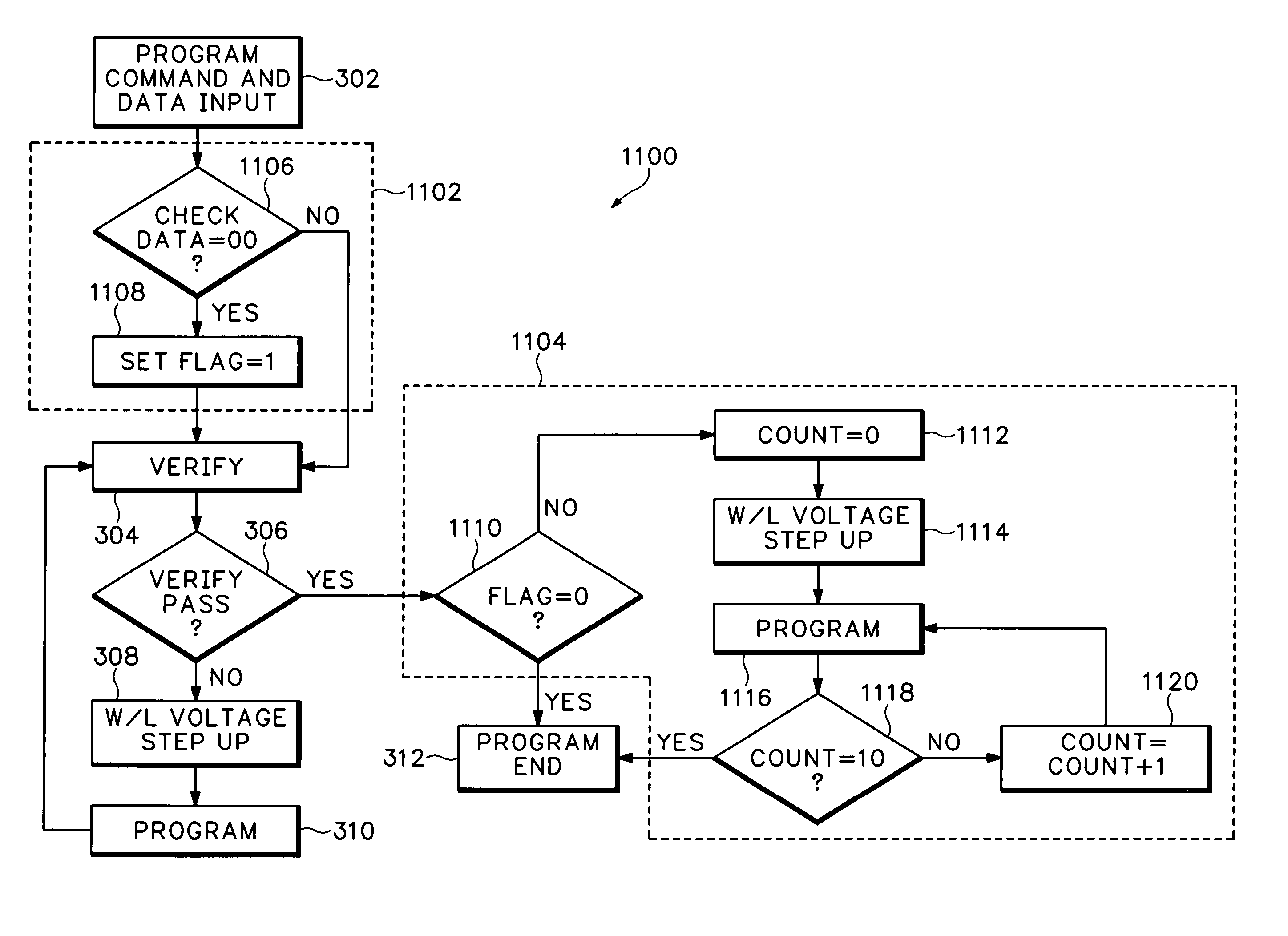
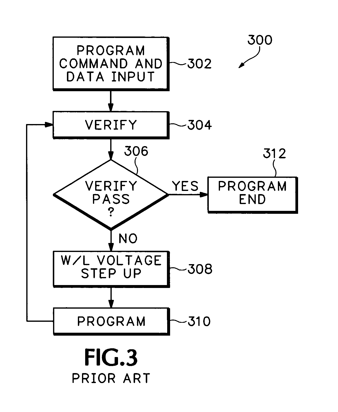
[0033]FIG. 3 is a flowchart of a programming method 300 associated with multi bit memory cells. Referring to FIGS. 1 and 3, the method 300 includes receiving a programming command and data at 302 instructing the memory device to program or store the data into the memory cell array 100. A programming word line voltage W / L is applied to the gate 11 responsive to the programming command that alters the charge stored in the floating gate 21 according to the data. At 304, the method 300 verifies successful programming by applying a fixed verify voltage at the gate 11 and comparing the threshold voltage Vt, a drain current Id, and / or the charge stored in the floating gate 21 to a reference memory cell.

[0034]If the verify operation fails at 306, the method 300 steps up the programming word line voltage W / L at 308, receives the programming command and data at 310, and re-verifies proper cell programming at 304. The charge stored in the floating gate 21 increases with each application of a p...


PUM


Abstract

We describe a multi level flash memory device and program method. The multi level flash memory device includes a plurality of memory cells, each storing an amount of charge indicative of more than two possible states and control circuitry coupled to the memory cells. The control circuitry to applying a programming voltage alternating with a verification voltage to the memory cells until all are at a desired state and applying at least one additional programming voltage to the cells in a highest state without applying a verification voltage. The method includes applying at least one programming pulse to the cells, verifying that each cell has reached the desired state, selecting the cells that are programmed for a highest state, and applying at least one additional programming pulse to the selected cells without further verifying their state.

Description

[0001]This application claims priority from Korean patent application number P2004-12984 filed Feb. 26, 2004, which we incorporate here by reference.FIELD[0002]This invention relates to a memory device and program method and, more particularly, to a multi level flash memory device and program method.BACKGROUND[0003]Modern computer systems often include nonvolatile semiconductor memory devices for data storage. Popular types of nonvolatile semiconductor memory devices are flash memory devices. Referring to FIG. 1, flash memory devices include an array 100 of flash memory cells 10. Each flash memory cell may be, e.g., a field effect transistor (FET). The flash memory cell 10 has a gate 11, a floating gate 21, a source 31, and a drain 41. The gate 11 operates responsive to a word line, e.g., word lines W / L0, W / L1, . . . , W / L1023. The source 31 is coupled to a sense line S / L. The drain 41 operates responsive to corresponding bit lines, e.g., bit lines B / L0, B / L1, . . . , B / L511.[0004]T...

Claims


Application Information

Patent Timeline
Patent Type & Authority Patents(United States)
IPC IPC(8): G11C11/34G11C16/06G11C16/00G11C11/56G11C16/10G11C16/34
CPCG11C11/5628G11C16/10G11C16/3459G11C16/3454G11C2211/5621G04B19/08G04B35/00
Inventor LEE, SEUNG-KEUNPARK, DONG-HO
Owner SAMSUNG ELECTRONICS CO LTD
Why Eureka
Try Eureka