Programmable CPU/interface buffer structure using dual port RAM

a buffer structure and interface technology, applied in the field of digital data processing systems and methods, can solve the problems of reducing the amount of time that the cpu can spend on other tasks, affecting the use of dma, and reducing the effective mips (millions of instructions per second) of the cpu, so as to achieve selectively enable buffers

Inactive Publication Date: 2006-05-30
NOKIA MOBILE PHONES LTD +1
View PDF18 Cites 19 Cited by
  • Summary
  • Abstract
  • Description
  • Claims
  • Application Information

AI Technical Summary

Benefits of technology

[0005]Disclosed is a programmable buffer circuit for interfacing a CPU to a plurality of channel interfaces. The buffer circuit includes a dual port memory having a first port coupled to a CPU data bus and a second port coupled to a channel data bus that serves the plurality of channel interfaces. The buffer circuit further includes an arbitrator for arbitrating access to the dual port memory by individual ones of the channel interfaces over the channel data bus; an address generator for generating dual port memory addresses for reading and writing data using the CPU data bus and the channel data bus; and a contr

Problems solved by technology

As can be appreciated, the use of programmed I/O consumes CPU bandwidth, and thus reduces the amount of time that the CPU can spend on other tasks.
This results in a decrease of the effective MIPS (millions of instruct

Method used


Image

  • Programmable CPU/interface buffer structure using dual port RAM
  • Programmable CPU/interface buffer structure using dual port RAM
  • Programmable CPU/interface buffer structure using dual port RAM

Examples


Embodiment Construction

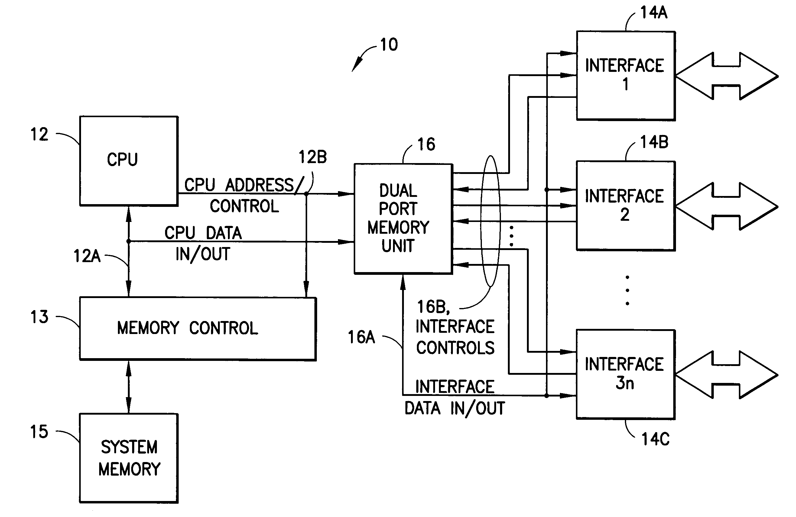
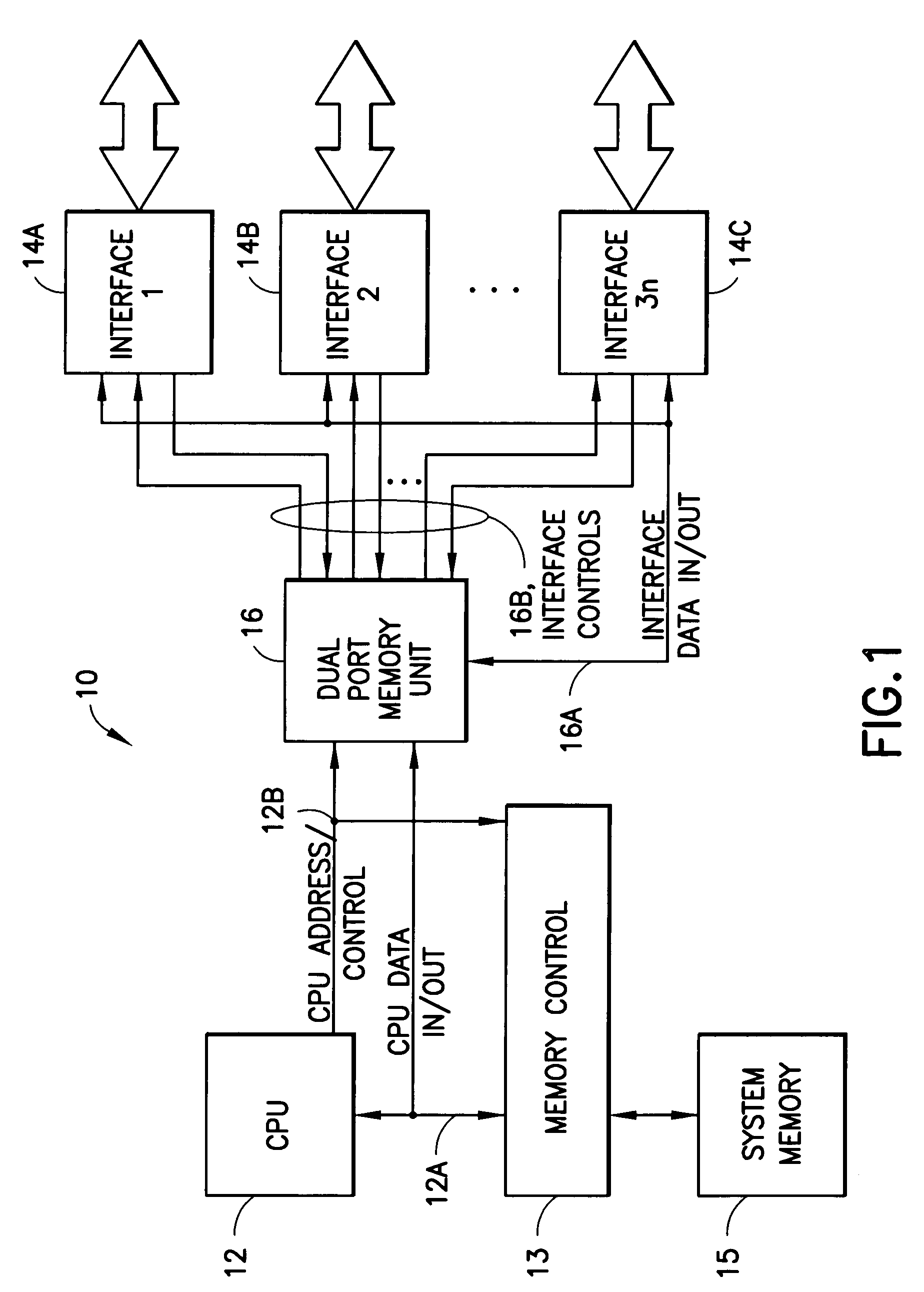
[0019]FIG. 1 is an overall block diagram of a data processing system (DPS) 10 constructed in accordance with the teachings of this invention. The DPS 10 includes at least one CPU 12, a plurality of Interface (IF) units 14A, 14B, . . . , 14C, referred to collectively as the IF 14, for coupling to external devices and buses, a dual port memory unit (DPMU) 16 that is constructed and operated in accordance with the teachings herein, a system memory control unit 13 and a system memory 15. While these various circuits and logical blocks can be provided as discrete components, in the presently preferred embodiment many or all of these components are integrated within an integrated circuit package, such as one or more Application Specific Integrated Circuit (ASIC) packages, as will be discussed in detail below. Other types of technologies could be used as well for implementing and embodying these teachings, such as Field Programmable Gate Array (FPGA) and Complex Programmable Logic Device (...


PUM


Abstract

Disclosed is a programmable buffer circuit (16) for interfacing a CPU (12) to a plurality of channel interfaces (14). The buffer circuit includes a dual port memory (18) having a first port coupled to a CPU data bus and a second port coupled to a channel data bus that serves the plurality of channel interfaces. The buffer circuit further includes an arbitrator (24) for arbitrating access to the dual port memory by individual ones of the channel interfaces over the channel data bus; an address generator (26) for generating dual port memory addresses for reading and writing data using the CPU data bus and the channel data bus; and a control unit (20) and allocator (22) that are programmable by the CPU for specifying individual ones of buffer locations and sizes within the dual port memory for individual ones of the channel interfaces, and for enabling and disabling individual ones of the buffers.

Description

FIELD OF THE INVENTION[0001]This invention relates generally to digital data processing systems and methods and, more particularly, relates to data buffering circuits and methods for use in digital data processing systems.BACKGROUND OF THE INVENTION[0002]It is common practice in the design of a data processing system with multiple interfaces, such as Ethernet, UART, CODEC, I2C Bus, etc., interfaces, to provide a data buffer, such as a first in / first out (FIFO) buffer, within each of the interface circuits. In this case data is transferred between system memory and the interface circuit buffers by the use of direct memory access (DMA) techniques, or by a central processor unit (CPU) performing read or write operations to remove data from the buffers or to store data in to the buffers. This latter process is sometimes referred to as “programmed I / O”.[0003]As can be appreciated, the use of programmed I / O consumes CPU bandwidth, and thus reduces the amount of time that the CPU can spend...

Claims


Application Information

Patent Timeline
IPC IPC(8): G06F13/36G06F13/28G06F5/06G06F5/10G06F13/00G06F13/38
CPCG06F5/10G06F5/065
Inventor ZHAO, SHENGARIES, WONGLIN, MING-HUI
Owner NOKIA MOBILE PHONES LTD
Why Eureka
Try Eureka