Semiconductor device package and method of manufacture

a semiconductor and device technology, applied in the field of packaging a semiconductor device, can solve the problems of difficult adhesive application in either form, long cure time of adhesive, damage to delicate die surface,

Active Publication Date: 2006-06-06
STMICROELECTRONICS ASIA PACIFIC PTE
View PDF15 Cites 8 Cited by
  • Summary
  • Abstract
  • Description
  • Claims
  • Application Information

AI Technical Summary

Benefits of technology

[0035]In accordance with another embodiment of the invention, a semiconductor device is provided that includes a substrate having a semiconductor die attached thereto; a housing have a sidewall surrounding an open interior that is in communication with a first open end and with a second end that is closed in the sidewall, the first open end sized and shaped to circumscribe the channel, the second end having an opening formed therein to enable fluid communication with the open interior; and a molding material affixed to the substrate and to the housing to hold the housing in place and to seal the housing to the substrate to prevent fluid communication between the sidewall of the housing and the substrate.
[0036]In accordance with a further embodiment of the invention, a semiconductor device is provided that includes a substrate having a semiconductor die attached to a surface thereof; a housing having a sidewall surrounding an open interior that is in communication with a first open end and a second open end of the sidewall, the first open end sized and shaped to circumscribe the semiconductor die; an adaptor configured to be received in the second open end of the housing and to expose an active portion of the semiconductor die to at least one of light, fluid, fluid pressure, and fluid temperature without damaging or altering the semiconductor die adjacent the active area of the semiconductor die; and molding material affixed to the substrate and the housing to hold the housing in place and to seal the housing to the substrate to prevent fluid communication between the sidewall and the substrate.

Problems solved by technology

However, the application of adhesive in either form is difficult, prone to result in adhesive being erroneously applied to the die surface and requires lengthy periods for the adhesive to cure.
However, there is a risk that the delicate die surface can be damaged by the insert either at the preparation or the removal stage.
Insertion and removal are also additional steps in the manufacturing process that require more time, additional machinery, and increase the opportunity for error.

Method used


Image

  • Semiconductor device package and method of manufacture
  • Semiconductor device package and method of manufacture
  • Semiconductor device package and method of manufacture

Examples


Embodiment Construction

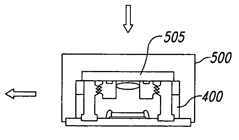
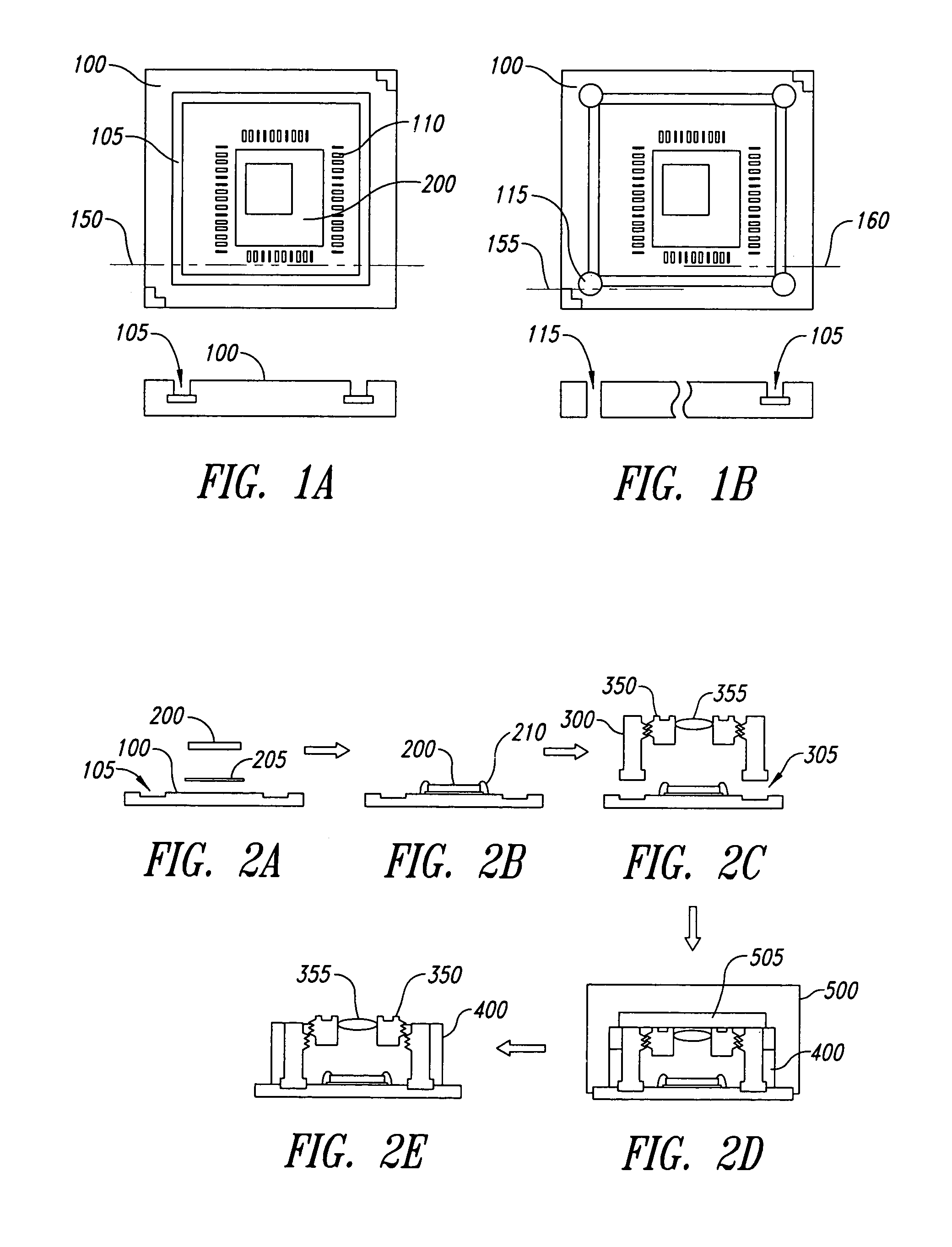
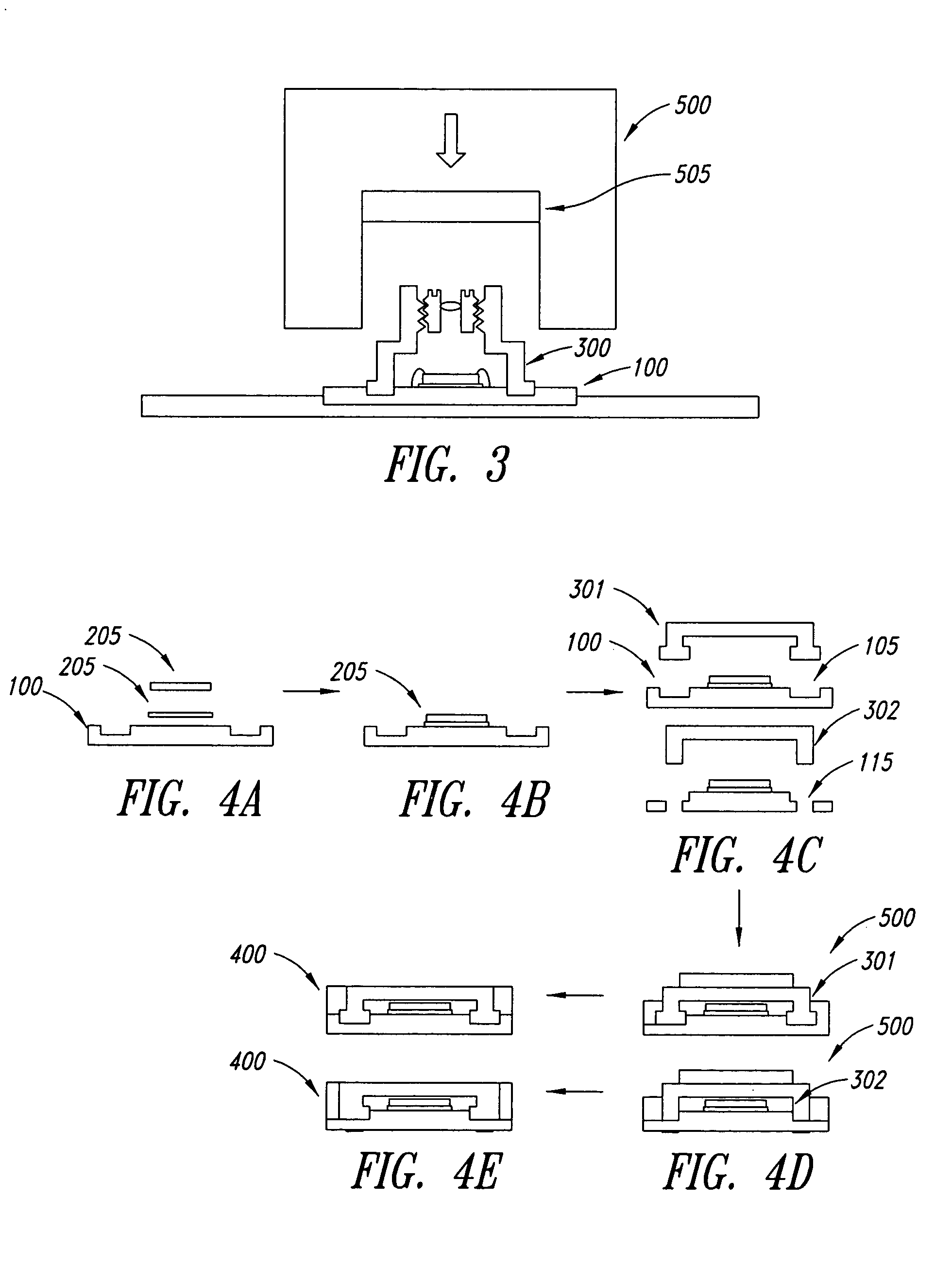
[0057]FIG. 1A shows a top plan and side view of a substrate 100 including an attached semiconductor die 200. The substrate is preferably composed of an epoxy material such as FR4 / 5 or BT. The semiconductor die 200 is attached to the surface of the substrate using a suitable adhesive such as an epoxy based adhesive. Immediately surrounding the semiconductor die 200 is a series of electrical contact pads 110. The pads 110 are arranged to be electrically connected in a manner that ultimately allows electrical signals to be sent and received by the semiconductor die. The pads may, for instance, be connected to a series of solder balls on the lower surface of the substrate that are arranged to allow the package to be secured to a circuit board. Toward the outer edge of the substrate 100 surface, outside the pads 110, is a shallow channel 105. This channel 105 is intended to receive the lower surface of a housing part, which is added to enclose the semiconductor die 200. The side view of ...


PUM

PropertyMeasurementUnit
pressureaaaaaaaaaa
temperatureaaaaaaaaaa
adhesiveaaaaaaaaaa

Abstract

A semiconductor package having a substrate; a semiconductor die attached to the substrate; a housing attached to the substrate and arranged to surround the semiconductor die; and solidified molding material arranged around the housing and adhering to the substrate to secure the housing in position on the substrate. A method of manufacturing the package is also disclosed.

Description

BACKGROUND OF THE INVENTION[0001]1. Field of the Invention[0002]The present invention relates to a method of packaging a semiconductor device. It finds particular utility with devices such as image sensors, MEMs, and pressure sensors.[0003]2. Description of the Related Art[0004]Semiconductor sensor packages generally include a semiconductor die part that is mounted on a substrate made of metal or plastic or a combination thereof, with the die and substrate being enclosed within a plastic material. However, since sensor semiconductors must be capable of being exposed to, e.g., light, in the case of optical sensors, or a fluid, in the case of pressure sensors, the active die surface must be left exposed, or at least accessible, after the die and substrate have been enclosed.[0005]Prior art packaging techniques often use a ceramic substrate material, which is preconfigured with a cavity to accept the die. Such ceramic substrates are in single unit form, they cost more than substrates m...

Claims


Application Information

Patent Timeline
Patent Type & Authority Patents(United States)
IPC IPC(8): H01L21/44H01L23/28G01L9/00H01L23/02H01L23/04H01L23/473H01L31/0203H01L31/0232H01L31/024
CPCB81C1/00269G01L19/143H01L23/04H01L23/473H01L24/97H01L2224/83101H01L2924/01024H01L2924/01027H01L2924/01029H01L2924/01077H01L2924/01078H01L2924/01079H01L2924/01006H01L2924/01005H01L23/3135H01L2924/15787H01L2924/181
Inventor LOO, KUM-WENGKHO, CHEK-LIM
Owner STMICROELECTRONICS ASIA PACIFIC PTE
Why Eureka
Try Eureka