Semiconductor device and method of manufacturing the same

a semiconductor device and semiconductor technology, applied in the direction of semiconductor devices, basic electric elements, electrical equipment, etc., can solve the problems of limited operation range of n channel type high sustaining voltage mos transistors, insufficient improvement of conventional semiconductor devices in sustaining voltage, and difficult operation at all over the rang

Inactive Publication Date: 2006-06-06
SEMICON COMPONENTS IND LLC
View PDF14 Cites 8 Cited by
  • Summary
  • Abstract
  • Description
  • Claims
  • Application Information

AI Technical Summary

Benefits of technology

[0019]A semiconductor device of the invention has a gate electrode formed extending on a first and second gate insulation films formed on first conductive type semiconductor substrate, a second conductive type source region adjacent to one end of said gate electrode, a first low concentration second conductive type drain region formed facing said source region through a channel region, having high impurity concentration peak at a position of the predetermined depth at least in said substrate under said first gate insulation film, and formed so that high impurity concentration becomes low at a region near surface of the substrate, a second concentration second conductive type drain region formed so as to range to the first low concentration second conductive type drain region, and a third concentration second conductive type drain region separated from the other end of said gate electrode and included in said second concentration second conductive type drain region.

Problems solved by technology

Thus, operation range of the N channel type high sustaining voltage MOS transistor is limited and operation at all over the range is difficult.
Although it is considered to increase ion implantation volume (dose) and to rise concentration of N− type drain region as shown in FIG. 9 to improve operation sustaining voltage (VSUS), the conventional semiconductor device is not improved enough in sustaining voltage as shown with white circles.
Therefore, there is not effective means improving operation sustaining voltage.

Method used


Image

  • Semiconductor device and method of manufacturing the same
  • Semiconductor device and method of manufacturing the same
  • Semiconductor device and method of manufacturing the same

Examples


first embodiment

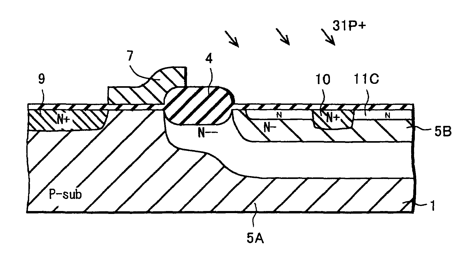
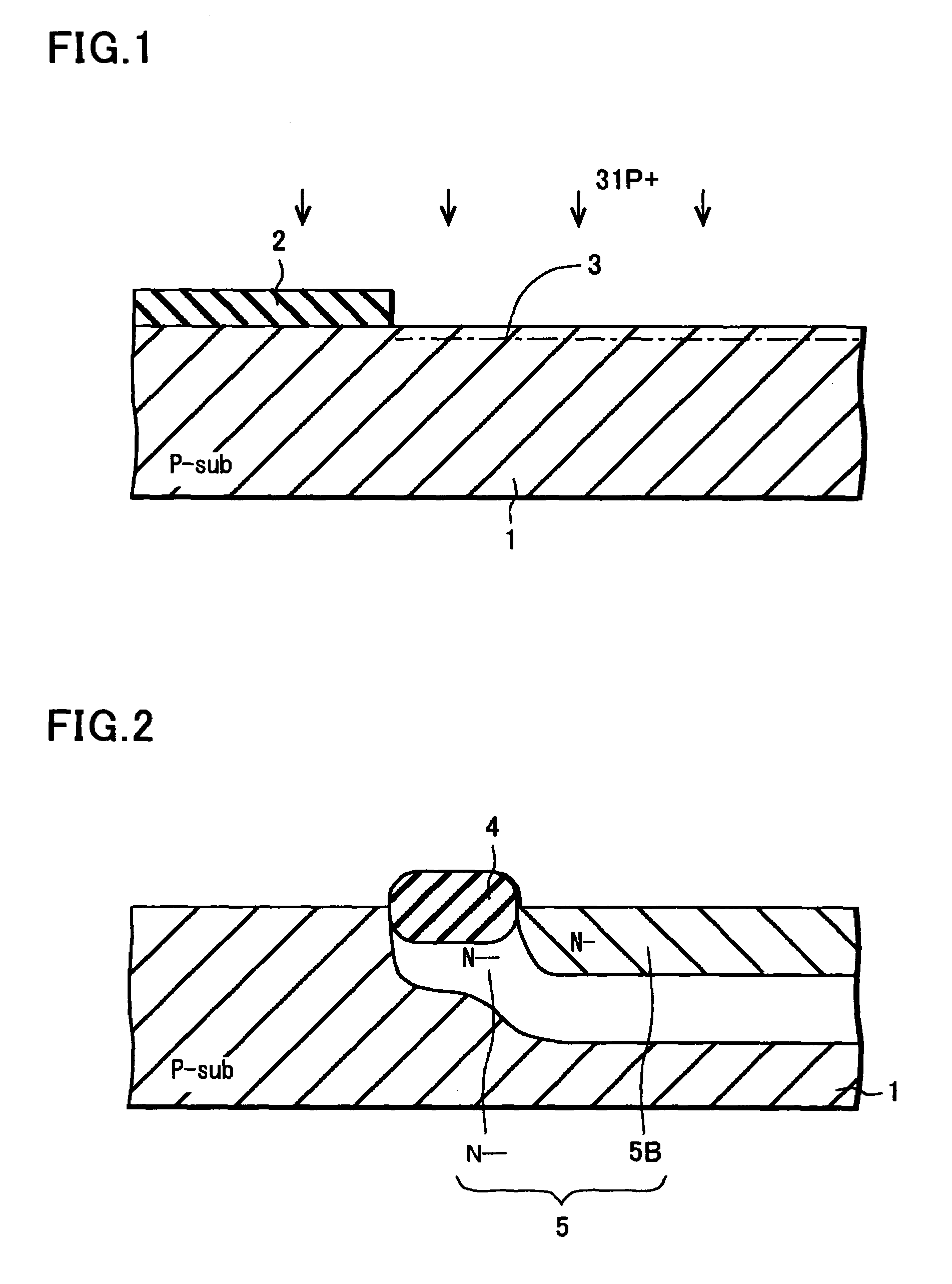
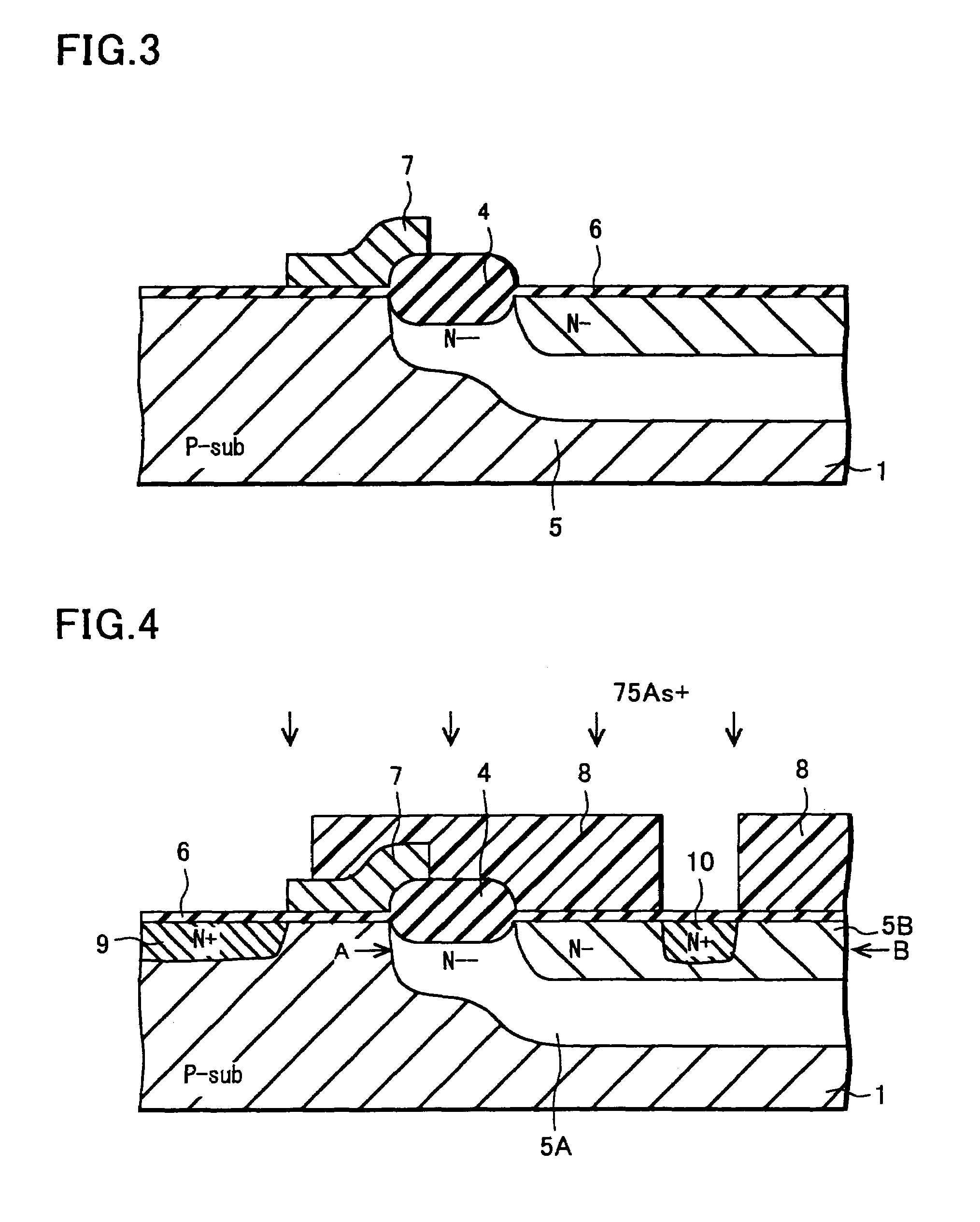
[0047]In a semiconductor device of a first embodiment according to the invention, a first gate insulation film 4 and a second gate insulation film 6 are formed on first conductive type semiconductor substrate, for example, P type semiconductor substrate (P-SuB) 1, and a first gate insulation 4 is formed so as to span from the first gate insulation film 4 to the second gate insulation film 6 as FIG. 4. A high concentration second conductive (N+) type source region 9 is formed so as to be adjacent to one end of said first gate insulation 4, a first low concentration second conductive (N−) type drain region 5A is formed so as to face said source region 9 through a channel region under the first gate insulation 4, a second low concentration second conductive (N−) type drain region 5B is formed so as to range to the first low concentration second conductive (N−) type drain region 5A, and further, a high (third) concentration second conductive (N+) type drain region 10 is formed so as to ...

third embodiment

[0064]Next, the invention will be described.

[0065]The characteristic of the semiconductor device of the third embodiment is that a middle concentration N type layer 11A is formed having the predetermined space (L) from one end portion (drain side) of the first gate insulation 4 through said first gate insulation film 4 as shown in FIG. 10. Since electric field concentration at the end portion of the first gate electrode 7 by forming the N type layer 11A having the predetermined space (L) from one end portion the gate gate electrode 7, higher sustaining voltage is designed.

second embodiment

[0066]In the above-mentioned method of manufacturing the semiconductor device, in the process of FIG. 6 described at the above-mentioned second embodiment, a middle concentration N type layer 11A is formed near the N+ type drain region 10 included in said N− type drain region having the predetermined space (L) from one end portion of said first gate insulation 4 as shown in FIG. 10 by ion-implanting phosphorus ion (31P+), for example, with about 160 KeV in acceleration voltage and about 2×10¹² / cm2 in implantation dose forming a photo-resist 12 so as to overlap with the predetermined space from the one end portion (drain side) of the gate electrode. Therefore, a space from the first gate insulation 4 (L) can be set freely by adjusting overlap quantity to the gate electrode 7 through the first gate insulation film 4 at forming the photo-resist 12.

[0067]An another embodiment forming the above-mentioned middle concentration N type layer having the predetermined space from one end (drain...


PUM


Abstract

A semiconductor device has a gate electrode formed extending on a first and second gate insulation films formed on P type semiconductor substrate, an N+ type source region adjacent to one end of the gate electrode, an N− type drain region facing said source region through a channel region, having high impurity concentration peak at a position of the predetermined depth at least in said substrate under said first gate insulation film, and formed so that high impurity concentration becomes low at a region near surface of the substrate, an N− type drain region formed so as to range to the N− type drain region, an N+ type drain region separated from the other end of said gate electrode and included in said N− type drain region, and an N type layer formed so as to span from one end portion of said first gate insulation film to said N+ type drain region.

Description

BACKGROUND OF THE INVENTION[0001]1. Fieled of the Invention[0002]The present invention relates to a semiconductor device and a method of manufacturing the device, particularly to technique improving operation sustaining voltage characteristic of high sustaining voltage MOS transistor for high voltage of power source (HV-VDD) used for an LCD driver, an EL driver and so on.[0003]2. Description of the Related Art[0004]A semiconductor device according to the related art will be described below referring a section view of an LDD type high sustaining voltage MOS transistor shown in FIG. 13.[0005]In FIG. 13, a gate electrode 53 is formed on a P type semiconductor substrate (P-Sub) 51 through a gate insulation film 52. An N+ type source region 54 is formed so as to be adjacent to one end of said gate electrode 53, an N− type drain region 56 is formed facing said source region 54 through a channel region and further separated from the other end of the gate electrode 53, and an N+ type drain ...

Claims


Application Information

Patent Timeline
Patent Type & Authority Patents(United States)
IPC IPC(8): H01L21/336H01L21/265H01L29/78
CPCH01L29/7835H01L29/66659H01L21/26586H01L29/42368H01L29/0847H01L29/78
Inventor KIKUCHI, SHUICHINISHIBE, EIJISUZUKI, TAKUYA
Owner SEMICON COMPONENTS IND LLC
Why Eureka
Try Eureka