Supercharge Your Innovation With Domain-Expert AI Agents!

Shallow trench isolation polish stop layer for reduced topography

a technology of polish stop layer and trench isolation, which is applied in the direction of basic electric elements, semiconductor/solid-state device manufacturing, electric devices, etc., can solve the problems of unsatisfactory step formation between the sti feature and the barrier oxide layer, step contributes to undesirable thickness variations in the surface topography, and the photoresist layer used in the photolithography process to form precise lines is adversely affected by the surface topography

Inactive Publication Date: 2006-06-06
GLOBALFOUNDRIES INC
View PDF10 Cites 8 Cited by
  • Summary
  • Abstract
  • Description
  • Claims
  • Application Information

AI Technical Summary

Benefits of technology

The invention is a method for making a shallow trench isolation feature on a semiconductor substrate. The method includes steps of forming a polish stop layer, a nitride containing layer, and a shallow trench layer through a portion of the nitride containing layer and a portion of the polish stop layer. The shallow trench layer and the polish stop layer are then planarized until they are co-planar. The invention also includes a shallow trench isolation feature that includes a polish stop layer and a shallow trench layer that are co-planar. The technical effect of this invention is to provide a more reliable and effective shallow trench isolation feature that improves the performance and reliability of semiconductor devices.

Problems solved by technology

That is, an undesirable step is formed between the STI feature and the barrier oxide layer.
The step contributes to undesirable thickness variations in the surface topography of layers formed subsequently.
For example, a photoresist layer used in a photolithography process to form precise lines is adversely affected by the topography of the surface.
Accordingly, the operability of the device is adversely affected.
Further, the reliability and lifetime of the semiconductor device may be degraded.

Method used


Image

  • Shallow trench isolation polish stop layer for reduced topography
  • Shallow trench isolation polish stop layer for reduced topography
  • Shallow trench isolation polish stop layer for reduced topography

Examples


Embodiment Construction

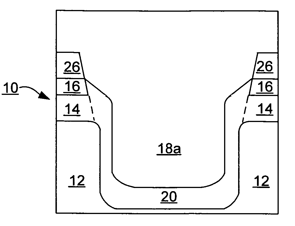
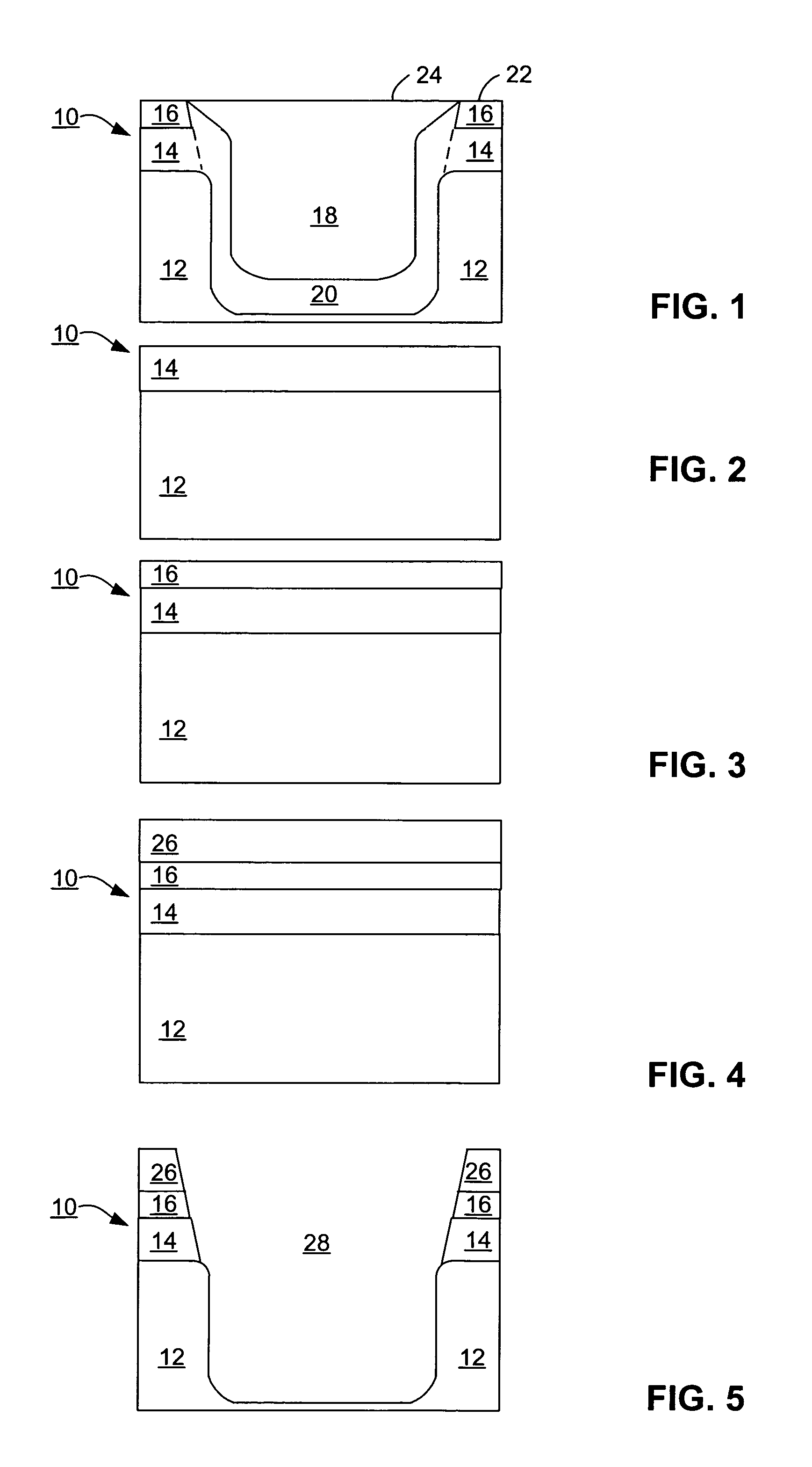
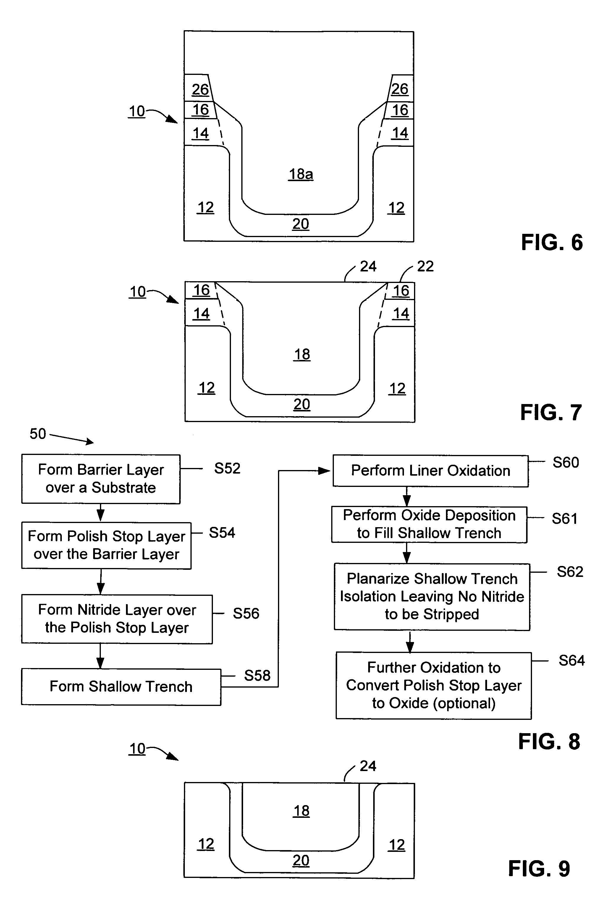
[0015]With reference to FIG. 1, an STI feature of the present invention is shown generally designated as 10. The STI feature 10 includes a semiconductor substrate 12 having a barrier layer 14 formed thereon. A polish stop layer 16 is formed over the barrier layer 14. An STI layer 18 (trench oxide) is formed through a portion of the polish stop layer 16, a portion of the barrier layer 14 and a portion of the semiconductor substrate 12. A liner layer 20 is interposed between the STI layer 18 and the semiconductor substrate 12 and the layers formed thereon, i.e., the barrier layer 14 and the polish stop layer 16. A surface 22 of the polish stop layer 16 and a surface 24 of the STI layer 18 are co-planer. Layers of materials used in the fabrication of semiconductor devices may be formed over the co-planar surfaces and benefit therefrom. Further, semiconductor devices that are known in the art such as a field effect transistor (FET) may be formed on, in or over the substrate 12 between s...


PUM

PropertyMeasurementUnit
thicknessaaaaaaaaaa
thicknessaaaaaaaaaa
thicknessaaaaaaaaaa

Abstract

A method of making and shallow trench isolation feature including 1) providing a semiconductor substrate, 2) forming a polish stop layer over the semiconductor substrate, 3) forming a nitride containing layer over the polish stop layer, 4) forming a shallow trench layer through a portion of the nitride containing layer, a portion of the polish stop layer and a portion of the semiconductor substrate, 5) removing the nitride containing layer by a chemical mechanical polishing process, and 6) planarizing the shallow trench layer and the polish stop layer until a surface of the shallow trench layer and a surface of the polish stop layer are co-planar.

Description

TECHNICAL FIELD[0001]The present invention generally relates to shallow trench isolation (STI) features used to electrically isolate semiconductor devices. In particular, the present invention relates to an STI polish stop layer for reduced topography.BACKGROUND[0002]A pervasive trend in modern integrated circuit manufacture is to produce semiconductor devices, e.g., FETs, having feature sizes as small as possible. Many present processes employ features, such as gate electrodes and interconnects, which have less than a 0.18 μm critical dimension. As feature sizes continue to decrease, the size of the resulting semiconductor device, as well as the interconnect between semiconductor devices, also decreases. Fabrication of smaller semiconductor devices allows more semiconductor devices to be placed on a single monolithic semiconductor substrate, thereby allowing relatively large circuit systems to be incorporated on a single, relatively small die area. In some cases, these semiconducto...

Claims


Application Information

Patent Timeline
Patent Type & Authority Patents(United States)
IPC IPC(8): H01L21/76
CPCH01L21/76224
Inventor LYONS, CHRISTOPHER F.SUBRAMANIAN, RAMKUMAR
Owner GLOBALFOUNDRIES INC
Features
  • R&D
  • Intellectual Property
  • Life Sciences
  • Materials
  • Tech Scout
  • Unparalleled Data Quality
  • Higher Quality Content
  • 60% Fewer Hallucinations
Learn More