Semiconductor device including an electrical contact connected to an interconnection

Active Publication Date: 2006-06-13
FUJITSU SEMICON LTD
View PDF10 Cites 6 Cited by
  • Summary
  • Abstract
  • Description
  • Claims
  • Application Information

AI Technical Summary

Benefits of technology

[0006]An object of the present invention is to provide a semiconductor device and the method for fabricating the

Problems solved by technology

However, as the generations advance, this has found technical limitations.
However, in contacting an upper interconnection layer to a lower damascene i

Method used


Image

  • Semiconductor device including an electrical contact connected to an interconnection
  • Semiconductor device including an electrical contact connected to an interconnection
  • Semiconductor device including an electrical contact connected to an interconnection

Examples


Embodiment Construction

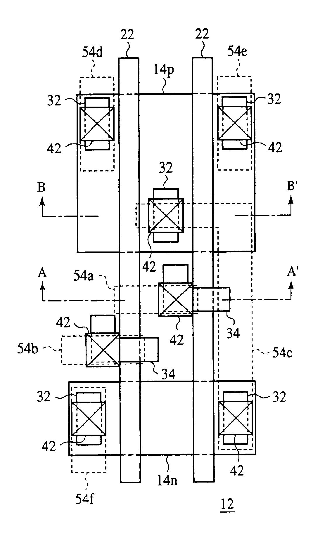
[0022][The Principle of the Present Invention]

[0023]As described above, in forming an electrical contact to be connected to an end part of a damascene interconnection, the defective contact often occurs between the damascene interconnection and the upper interconnection.

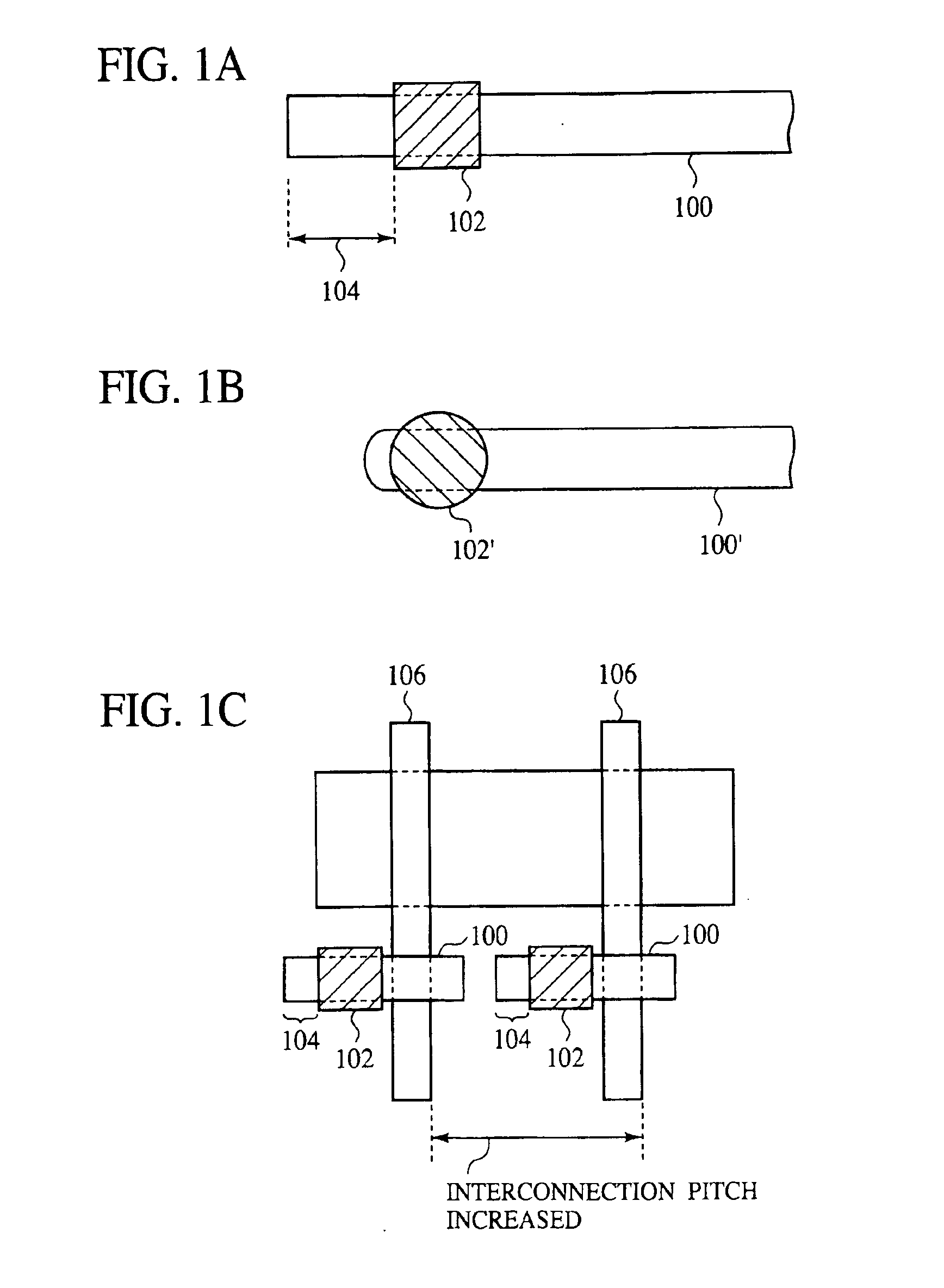
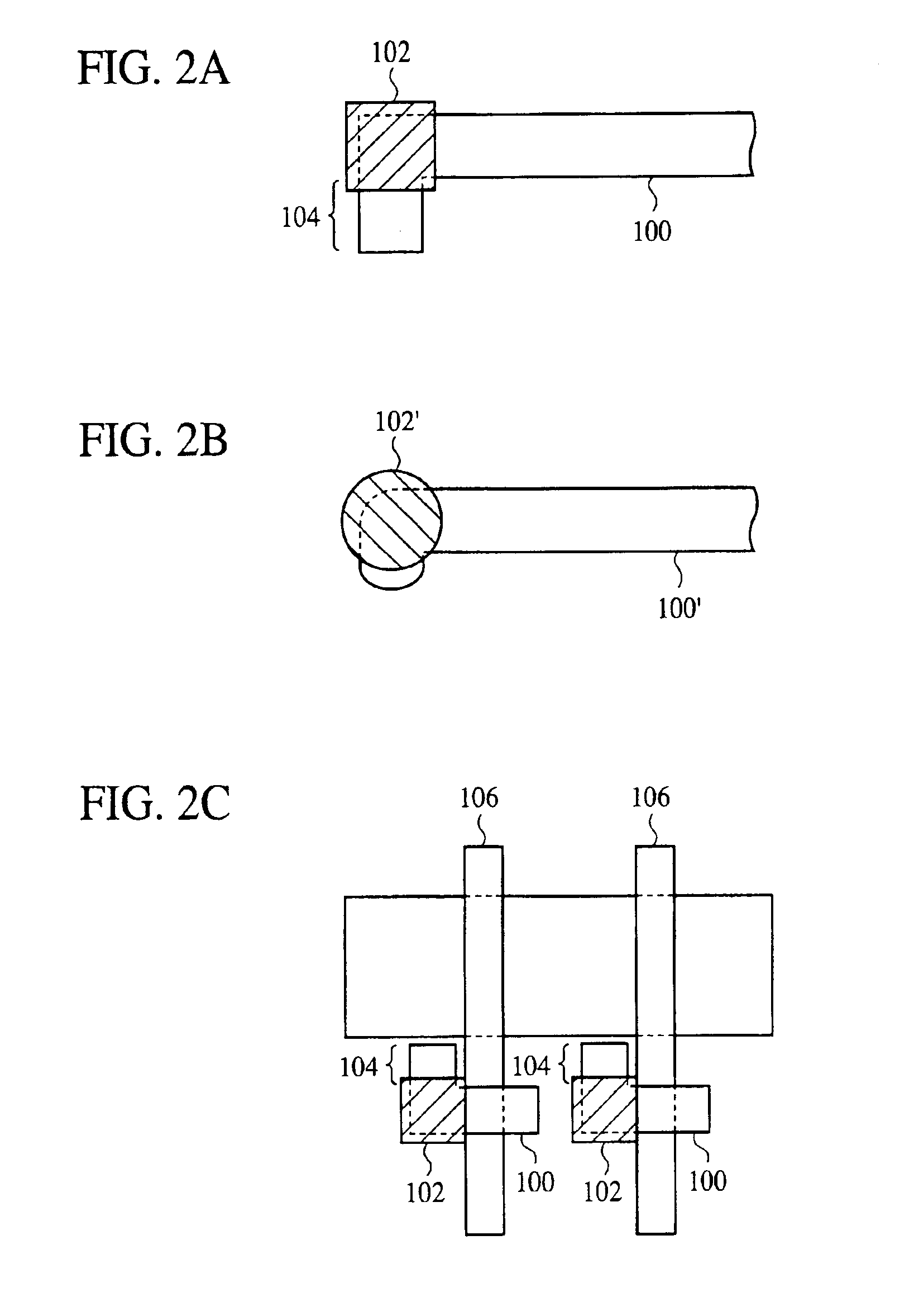
[0024]The inventor of the present invention has made earnest studies of causes of this problem and found that the proximity effect in the lithography step for forming an interconnection groove for a damascene interconnection to be buried in causes the problem. The proximity effect is more conspicuous in the pattern end part of a perforated pattern than in the pattern end part of a left pattern. In forming a groove-shaped perforated pattern to be used in forming an interconnection groove, a position of the pattern end is shrunk from a position of the design pattern due to the proximity effect. Accordingly, when a contact region is arranged to overlap the pattern end part of the design pattern, the end of the formed pa...


PUM


Abstract

The semiconductor device comprises an interconnection buried in an interconnection groove formed in a lower insulating film, and an upper insulating film having a contact hole formed down to an end part of the interconnection. The interconnection groove is formed by using a design pattern having a main interconnection portion 100 and an extended portion 104 provided at an end part of a main interconnection portion 100 for forming the interconnection and extended perpendicularly to an extending direction of the main interconnection portion 100.

Description

CROSS-REFERENCE TO RELATED APPLICATIONS[0001]This application is based upon and claims the benefit of priority from the prior Japanese Patent Application No. 2002-379569, filed on Dec. 27, 2002, the entire contents of which are incorporated herein by reference.BACKGROUND OF THE INVENTION[0002]The present invention relates to a semiconductor device and a method for fabricating the same, more specifically to a semiconductor device including an electrical contact connected to a damascene interconnection, and a method for fabricating the same.[0003]As semiconductor devices are larger-scaled and integrated higher, design rules of the interconnections are diminished as the generations. Conventionally, interconnections have been formed by depositing conducting materials and patterning the deposited conducting materials by lithography and dry etching. However, as the generations advance, this has found technical limitations. As a new process for forming the interconnections, which takes ove...

Claims


Application Information

Patent Timeline
IPC IPC(8): H01L23/52H01L21/3205H01L21/027H01L23/48H01L21/768H01L23/522H01L27/02
CPCH01L21/76838H01L23/5226H01L27/0203H01L2924/0002H01L2924/00H01L21/76895H01L23/528
Inventor TAKAO, YOSHIHIRO
Owner FUJITSU SEMICON LTD
Why Eureka
Try Eureka