Filter circuit with series and parallel elements

a filter circuit and series element technology, applied in the field of filter circuits, can solve the problems of limited difference between the center of the passband of the filter circuitry and the center of the stopband of the filter circuitry that needs large attenuation, and the difference between the center of the pass the center of the stopband of the filter circuitry that needs large attenuation, and achieve the effect of large attenuation

Inactive Publication Date: 2006-06-13
MITSUBISHI ELECTRIC CORP
View PDF16 Cites 9 Cited by
  • Summary
  • Abstract
  • Description
  • Claims
  • Application Information

AI Technical Summary

Benefits of technology

[0040]In accordance with the present invention, there is provided filter circuitry including a series element comprised of a resonance element having an antiresonance characteristic and a parallel element comprised of a series circuit having an inductor and a capacitor. The filter circuitry can thus have a low-loss wide-band pass filter characteristic even if a passband has a range of frequencies that is separated far apart from a range of frequencies of an attenuation band, and can also provide a large attenuation over a wide frequency band.

Problems solved by technology

Therefore, the difference between the center of the passband of the filter circuitry and the center of the stopband of the filter circuitry that needs large attenuation is limited by the performance of the used piezoelectric element.
A problem is therefore that the difference between the center of the passband of the filter circuitry and the frequency of an attenuation pole that provides large attenuation is only about 5 to 6% of the center of the passband of the filter circuitry.
Therefore, in the case where an inductor is included in each of the series element and parallel element of the filter circuitry as shown in FIG. 6, there is a problem that loss in the passband increases.
A further problem encountered with the prior art filter circuitry is therefore that because at a frequency within the passband the filter circuitry has an impedance having a component other than a pure resistance component, which increases with increase in the difference between the frequency and the antiresonance frequency fap, it is difficult to implement low-loss characteristics over a wide frequency band.
Another problem is therefore that while a wider-band characteristic can be implemented as compared with the filter circuitry including the SAW resonator 2, it is difficult to implement a low-loss pass filter characteristic.
A further problem is that because the q-factor of the resonance circuit 21 is small, it is difficult for the prior art filter circuitry to provide steeper attenuation at frequencies higher than the passband of the filter circuit, which is produced by the series element of the filter circuitry and it is difficult for the attenuation pole which the resonance circuit 21 forms to produce a steep zero point, so that the attenuation characteristic degrades in a frequency band higher than the passband of the filter circuitry.
In other words, a problem with prior art filter circuitry constructed as mentioned above is that when frequencies within the passband are away from those within the attenuation band, it is difficult to implement a low-loss wide-band pass filter characteristic and it is also difficult to provide a large attenuation over a wide frequency band.

Method used


Image

  • Filter circuit with series and parallel elements
  • Filter circuit with series and parallel elements
  • Filter circuit with series and parallel elements

Examples


embodiment 1

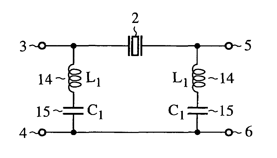
[0104]FIG. 9 is a block diagram showing filter circuitry according to embodiment 1 of the present invention. In the figure, reference numeral 2 denotes a SAW resonator (i.e., a resonator) having an antiresonance characteristic, the SAW resonator constituting a series element of the filter circuitry, reference numeral 3 denotes an input terminal, reference numeral 4 denotes a ground terminal disposed on an input side of the filter circuitry, reference numeral 5 denotes an output terminal, reference numeral 6 denotes a ground terminal disposed on an output side of the filter circuitry, reference numeral 14 denotes an inductor, and reference numeral 15 denotes a capacitor. Two series circuits each comprised of one inductor 14 and one capacitor 15 are parallel elements of the filter circuitry, and have a π-shaped circuit structure.

[0105]FIG. 10 is a circuit diagram showing an equivalent circuit of the filter circuitry that operates in a frequency range in which the SAW resonator 2 doesn...

embodiment 2

[0118]FIG. 15 is a block diagram showing filter circuitry according to embodiment 2 of the present invention, and FIG. 16 is an explanatory drawing for explaining an operation of the filter circuitry of FIG. 15. In the figure, reference numeral 2a denotes a first SAW resonator, reference numeral 2b denotes a second SAW resonator, reference numeral 27a denotes a pass filter characteristic of the first SAW resonator 2a, reference numeral 27b denotes a pass filter characteristic of the second SAW resonator 2b, and reference numeral 28 denotes a pass filter characteristic of the filter circuitry of FIG. 15.

[0119]The first SAW resonator 2a has a resonance frequency of frs1, an antiresonance frequency of fas1, and a capacitance of C2. The second SAW resonator 2b has a resonance frequency of frs2 an antiresonance frequency of fas2, and a capacitance of C3. The capacitance C2 of the first SAW resonator 2a is nearly equal to the capacitance C3 of the second SAW resonator 2b. The antiresonanc...

embodiment 3

[0125]FIG. 17 is an explanatory drawing for explaining an operation of filter circuitry according to embodiment 3 of the present invention. The filter circuitry that operates as shown in FIG. 17 has the same structure as the filter circuitry of FIG. 15. The inductance of each inductor 14, the capacitance of each capacitor 15, the capacitance C2 of a first SAW resonator 2a, and the capacitance C3 of a second SAW resonator 2b are determined so that a cutoff frequency fc and a frequency fn of an attenuation pole for each section 100a, which are determined by those components' values, become equal to those for any other section, as in the case of FIG. 16. The frequency fn of the attenuation pole is so set as to be lower than the antiresonance frequency fas1 of the first SAW resonator 2a and the antiresonance frequency fas2 of the second SAW resonator 2b.

[0126]Because a frequency difference between the attenuation pole caused by the antiresonance frequency fas1 of the first SAW resonato...


PUM


Abstract

Filter circuitry is provided with a series element and a parallel element. The filter circuitry transmits signals that fall within a certain passband and attenuates signals that don't fall within the certain passband. The series element is comprised of a resonance element having antiresonance characteristics, and the parallel element is comprised of a series circuit including an inductor and a capacitor.

Description

FIELD OF THE INVENTION[0001]The present invention relates to filter circuitry that transmits signals that fall within a certain passband for use with communication equipment and so on and that attenuates signals that don't fall within the certain passband.BACKGROUND OF THE INVENTION[0002]FIG. 1 is a block diagram showing prior art filter circuitry as described in Japanese patent application publication (TOKKAIHEI) No. 10-126212 (referred to as reference 1 from here on), for example. In the figure, reference numeral 1 denotes a SAW resonator that constitutes a parallel element, reference numeral 2 denotes a SAW resonator that constitutes a series element, reference numeral 3 denotes an input terminal, reference numeral 4 denotes a ground terminal disposed on an input side of the prior art filter circuitry, reference numeral 5 denotes an output terminal, and reference numeral 6 denotes a ground terminal disposed on an output side of the prior art filter circuitry.[0003]FIG. 2 is a blo...

Claims


Application Information

Patent Timeline
Patent Type & Authority Patents(United States)
IPC IPC(8): H03H9/54H03H9/64H03H7/01H03H9/58
CPCH03H7/0115H03H9/6483H03H7/1766H03H7/463H03H7/1758H03H7/0123
Inventor MISU, KOICHIROIBATA, KOJIMURAI, KOUJIYOSHIDA, KENJIYAMAGATA, KOUSAKUITOH, KENJIMURASE, ISAOKOSHINAKA, MASAO
Owner MITSUBISHI ELECTRIC CORP
Why Eureka
Try Eureka