Patterned vertically aligned liquid crystal display

a vertical alignment and liquid crystal display technology, applied in non-linear optics, instruments, optics, etc., can solve the problems of reducing affecting the image quality, and limiting the design of the electrode aperture, so as to improve the aperture ratio, improve the pixel alignment margin, and improve the pixel quality

Inactive Publication Date: 2006-06-13
SAMSUNG DISPLAY CO LTD
View PDF10 Cites 10 Cited by
  • Summary
  • Abstract
  • Description
  • Claims
  • Application Information

AI Technical Summary

Benefits of technology

[0009]It is an object of the present invention to provide an electrode pattern design which enables a bigger margin for pixel alignment.
[0010]It is another object of the present invention to provide a method for repairing high pixel defects.
[0011]It is yet another object of the present invention to increase an aperture ratio.

Problems solved by technology

These parts of the LCD appear black, degrading the picture quality.
This limits the design of the apertures of the electrodes.
Accordingly, it is hard to design an electrode pattern that allows a bigger margin for pixel alignment.
Further, in a ring gate structure, it frequently causes a high pixel defect, which leaves pixels continuously in a white state as a result of shorting the pixel electrodes with the data lines or the gate lines.
This problem is difficult to repair.

Method used


Image

  • Patterned vertically aligned liquid crystal display
  • Patterned vertically aligned liquid crystal display
  • Patterned vertically aligned liquid crystal display

Examples


first embodiment

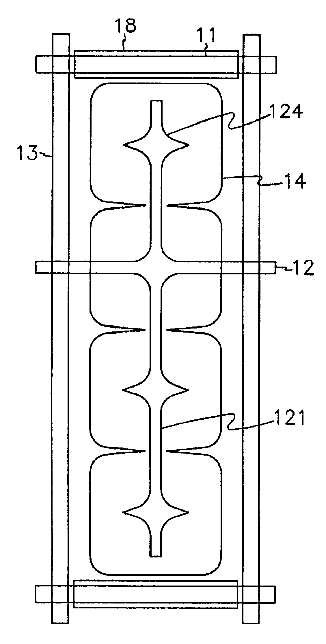
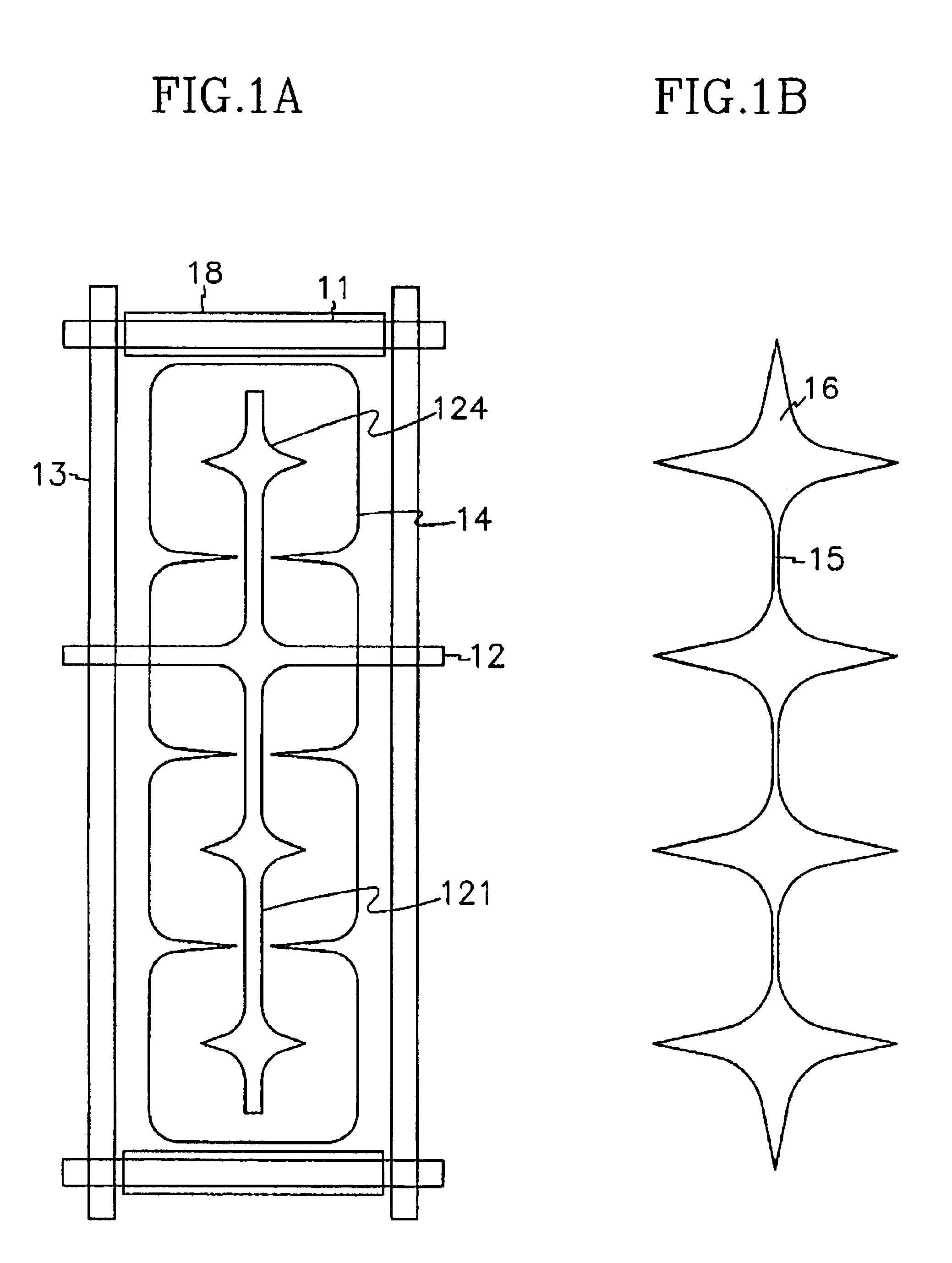
[0020]FIGS. 1A, 1B and 1C are partial layout views respectively of a lower substrate of a liquid crystal display (LCD), an aperture formed on an upper substrate of an LCD, and the two substrates in an assembled state according to the present invention. It is to be assumed that elements appearing in the drawings are provided over an entire surface of the substrates, and not just once or twice as shown in the drawings.

[0021]As shown in FIG. 1A, gate lines 11 and a storage line 12 extend in one direction on the lower substrate. A storage electrode 121 is formed perpendicular to the gate lines 11 and the storage line 12, the storage electrode 121 being branched from the storage line 12. The storage electrode 121 has projections 124 that are formed outwardly from the storage electrode 121 in a direction opposite to a longitudinal axis of the storage electrode 121. Adjacent projections 124 are formed at a uniform distance from each other. Although the storage line 12 comes to have the sam...

second embodiment

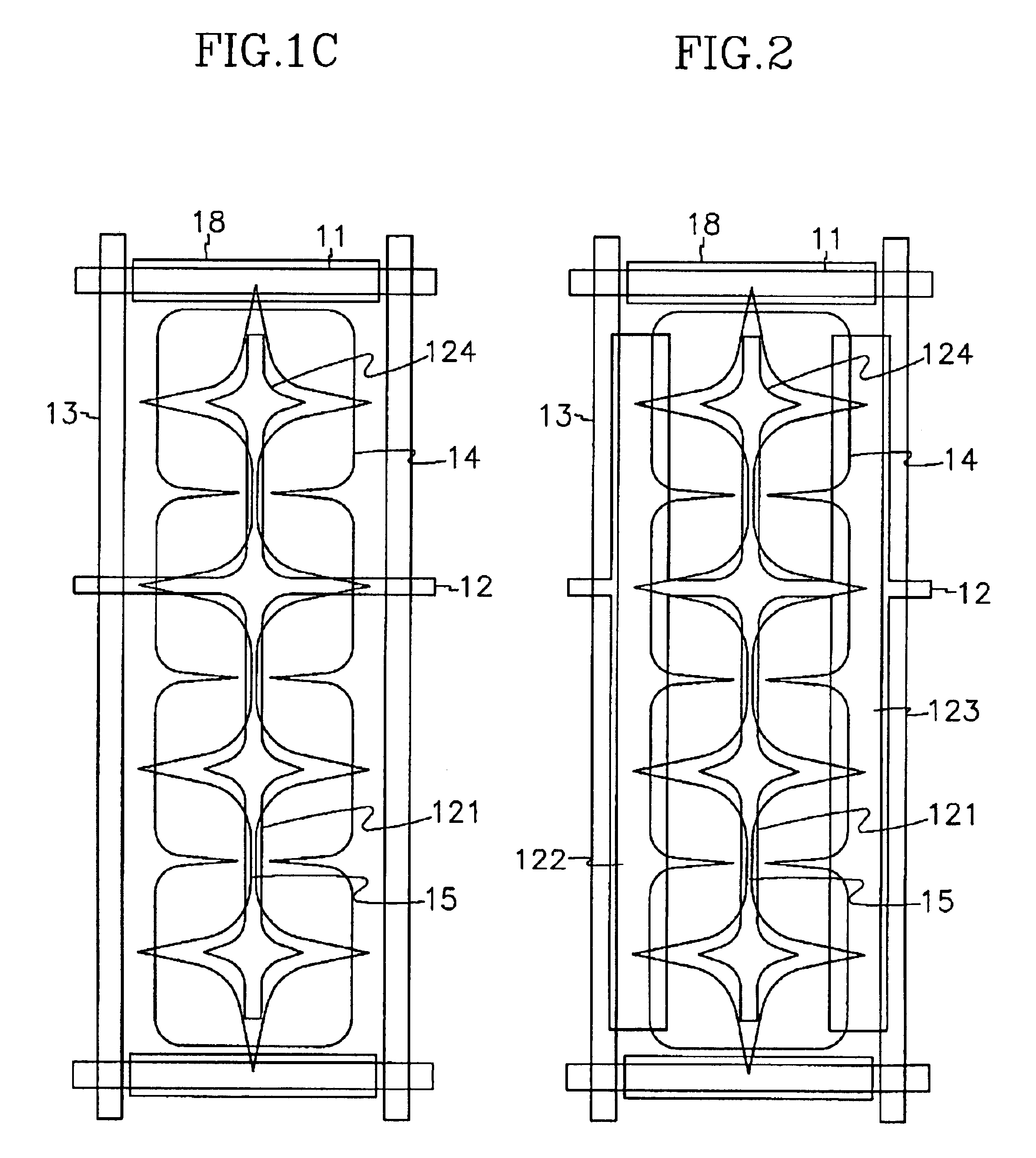
[0030]FIG. 2 is a partial plan view of an LCD according to the present invention.

[0031]In the second embodiment, the first cover pattern 122 and the second cover pattern 123, which are connected to the storage line 12, are additionally provided. These cover patterns are preferably made of the same material and at the same time as the gate lines and the storage lines. The first cover pattern 122 and the second cover pattern 123 preferably are provided partially covering the pixel electrodes 14 and the data lines 13 in an identical direction with the data lines 13. The first cover pattern 122 and the second cover pattern 123 ends before contacting the gate lines 11. The first cover pattern 122 and the second cover pattern 123 overlap with a part of the data lines 13 to increase a capacitance formed between the cover patterns 122 and 123 and the data lines 13.

[0032]The cover patterns 122 and 123 decrease the electric field between the data lines 13 and the common electrode to prevent t...

third embodiment

[0033]FIG. 3 is a partial plan view of an LCD according to the present invention.

[0034]The third embodiment is the same as the second embodiment except that the storage electrode 121 is removed.

[0035]When the storage line 12 and the cover patterns 122 and 123 can obtain enough storage capacitance, the aperture ratio is increased by not forming the storage electrode 121.

[0036]FIG. 4 is a partial plan view of an LCD according to a fourth embodiment of the present invention. The fourth embodiment is the same as the second embodiment except that the cover patterns 122 and 123 do not overlap any part of the pixel electrodes 14.

[0037]This can eliminate large variances in storage capacitance even if a misalignment occurs between a photo shot for forming the cover patterns 122 and 123 and a photo shot for forming the pixel electrodes 14. Accordingly, stitch defects are prevented.


PUM

PropertyMeasurementUnit
angleaaaaaaaaaa
electric fieldaaaaaaaaaa
transmittanceaaaaaaaaaa

Abstract

In a vertically aligned mode LCD, a gate line and a storage line are formed on a substrate in parallel, and a storage electrode and a cover pattern are formed as branches of the storage line. The storage electrode is overlapped with an aperture of a common electrode formed on an upper substrate. The cover pattern is located between a pixel electrode and a data line to prevent a light leakage. Accordingly, an alignment error margin of the upper substrate and the lower substrate is increased, an aperture ratio is enhanced, and repairing the high pixel defect is possible. Further, the light leakage caused by a voltage of the data line is prevented.

Description

[0001]This application is a continuation application of co-pending U.S. application Ser. No. 09 / 417,076, filed on Oct. 13, 1999, which has now become U.S. Pat. No. 6,577,366 B1.BACKGROUND OF THE INVENTION[0002](a) Field of the Invention[0003]The present invention relates to a liquid crystal display having a wide viewing angle, and more particularly, to a liquid crystal display of which viewing angle is made wide by patterning apertures in electrodes.[0004](b) Description of the Related Art[0005]Liquid crystal displays (LCDs) typically include two substrates and a liquid crystal layer interposed between the substrates. The transmittance of light is controlled by the intensity of an electric field applied to the liquid crystal layer.[0006]In a vertically aligned (VA) mode LCD, liquid crystal molecules take on a homeotropic orientation in which long axes of the molecules are perpendicular to the substrate. This configuration cuts off lights almost completely in an “off” state where an ...

Claims


Application Information

Patent Timeline
Patent Type & Authority Patents(United States)
IPC IPC(8): G02F1/13G02F1/1343G02F1/1333G02F1/1335G02F1/136G02F1/1362G02F1/139
CPCG02F1/133707G02F1/134336G02F1/136213G02F1/133512G02F1/134309G02F1/136259G02F2201/40G02F2001/134318G02F2001/136263G02F2001/136272G02F2201/122G02F2201/128G02F1/1393G02F1/134318G02F1/136263G02F1/136272G02F1/1343G02F1/136
Inventor KIM, KYEONG-HYEONLEE, KYE-HUNPARK, SEUNG-BEOMSONG, JANG-KUN
Owner SAMSUNG DISPLAY CO LTD
Why Eureka
Try Eureka