Optical scatterometry of asymmetric lines and structures

a technology of optical scatterometry and asymmetric lines, applied in the field of optical devices, can solve the problems of asymmetric lines and the inability to distinguish between right and left asymmetries

Active Publication Date: 2006-06-13
THERMA WAVE INC +1
View PDF25 Cites 154 Cited by
  • Summary
  • Abstract
  • Description
  • Claims
  • Application Information

AI Technical Summary

Problems solved by technology

However, a significant problem for both CD and overlay measurements with optical scatterometry is the problem of asymmetric lines.
The problem of asymmetric lines is that in most cases it is not possible to distinguish between right and left asymmetries with conventional optical scatterometry techniques without resort to special or multiple patterns.

Method used


Image

  • Optical scatterometry of asymmetric lines and structures
  • Optical scatterometry of asymmetric lines and structures
  • Optical scatterometry of asymmetric lines and structures

Examples


Embodiment Construction

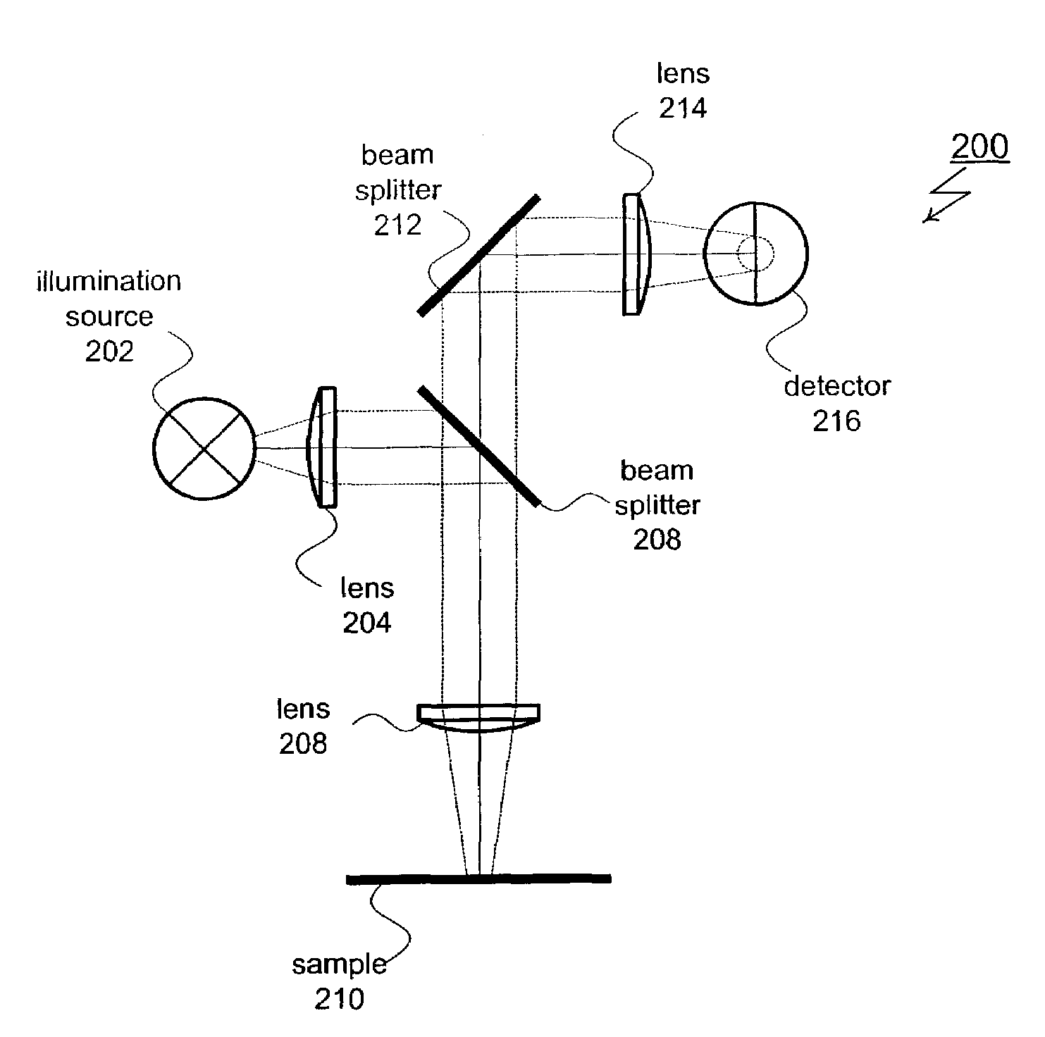
[0027]The present invention provides several methods for analyzing asymmetric structures (including isolated and periodic structures) included within semiconductor wafers. For one of these methods, an existing optical metrology system is enhanced to provide sensitivity to asymmetries. FIG. 2 shows a specific example of this type of enhancement applied to a broadband spectrometer 200. Spectrometer 200 includes an illumination source 202 that produces a polychromatic probe beam. For this particular implementation, the probe beam passes through a first lens 204, first beam splitter 208 and second lens 208 before reaching a subject 210. Subject 210 is typically a semiconductor wafer and typically includes an isolated or periodic two or three dimensional surface structure such a line, grating, via or pattern of vias. The polychromatic probe beam is reflected by subject 210 and directed through lens 208, first beam splitter 206, second beam splitter 212 and third lens 214 before reaching ...


PUM

PropertyMeasurementUnit
angleaaaaaaaaaa
angleaaaaaaaaaa
angle of attackaaaaaaaaaa

Abstract

A method for analyzing asymmetric structures (including isolated and periodic structures) includes a split detector for use in a broadband spectrometer. The split has detector has separate right and left halves. By independently measuring and comparing the right and left scattered rays, information about asymmetries can be determined.

Description

PRIORITY CLAIM[0001]This application claims priority from prior provisional applications Ser. No. 60 / 364,154, filed Mar. 13, 2002, and which is incorporated herein by reference.TECHNICAL FIELD[0002]The subject invention relates to optical devices used to non-destructively evaluate semiconductor wafers. In particular, the present invention relates to methods for measuring asymmetric lines and structures.BACKGROUND OF THE INVENTION[0003]In the past few years, there has been considerable interest in using optical scatterometry (i.e., diffraction) for performing critical dimension (CD) measurements of the lines and structures that comprise an integrated circuit. It has been shown that optical scatterometry from periodic two-dimensional structures (e.g. line gratings) and from three-dimensional structures (e.g. patterns of vias or mesas) can provide accurate and precise measurements of the spatial profiles of these various lines, vias and mesas. Various optical techniques can be utilized...

Claims


Application Information

Patent Timeline
Patent Type & Authority Patents(United States)
IPC IPC(8): G01B11/30G01B11/24G03F7/20
CPCG03F7/70633G03F7/70625
Inventor OPSAL, JONROSENCWAIG, ALLAN
Owner THERMA WAVE INC
Why Eureka
Try Eureka