
Data input and output circuits for multi-data rate operation

a data input and output circuit technology, applied in the field of memory devices, can solve the problems of increasing complexity of interconnection structures, increasing the difficulty of meeting timing requirements, and increasing the complexity of data input and output circuits to interface memory cells with device i/o pins

Inactive Publication Date: 2006-06-13
WINBOND SYST LAB
View PDF13 Cites 96 Cited by
  • Summary
  • Abstract
  • Description
  • Claims
  • Application Information

AI Technical Summary

Benefits of technology

[0019]The foregoing, together with other aspects of this invention, will become more ap

Problems solved by technology

As the number of I / O pins increases and the number of memory cells in the memory device grows, the interconnection structure also grows in complexity.
Moreover, the data input and output circuits to interface the memory cells to the device I / O pins become more complicated, particularly if the memory device is required to support a number of operating modes.
However, as the operating speed increases, it becomes more challenging to meet these timing requirements.
More complicated timing circuits are typically required to generate triggering signals for synchronous circuits within the memory device to ensure conformance with the input and output timing specifications.

Method used


Image

  • Data input and output circuits for multi-data rate operation
  • Data input and output circuits for multi-data rate operation
  • Data input and output circuits for multi-data rate operation

Examples


Embodiment Construction

[0032]For clarity, the invention is described for a specific implementation of a memory device. However, the specific details are intended to be illustrative, and not limitations, of the present invention. It will be recognized that alternative implementations of the invention and modifications of the circuits and architectures described herein can be made (e.g., to satisfy a particular design requirement), and these modifications and variations are within the scope of the invention.

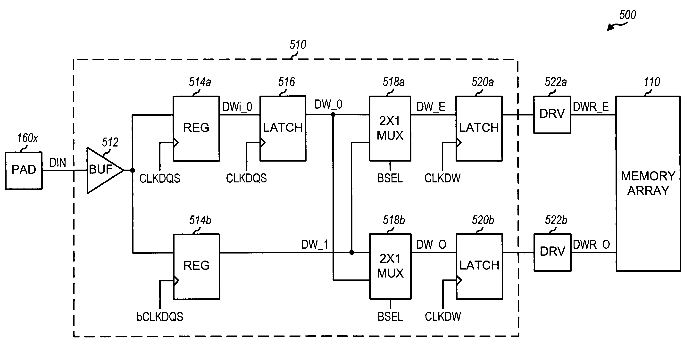
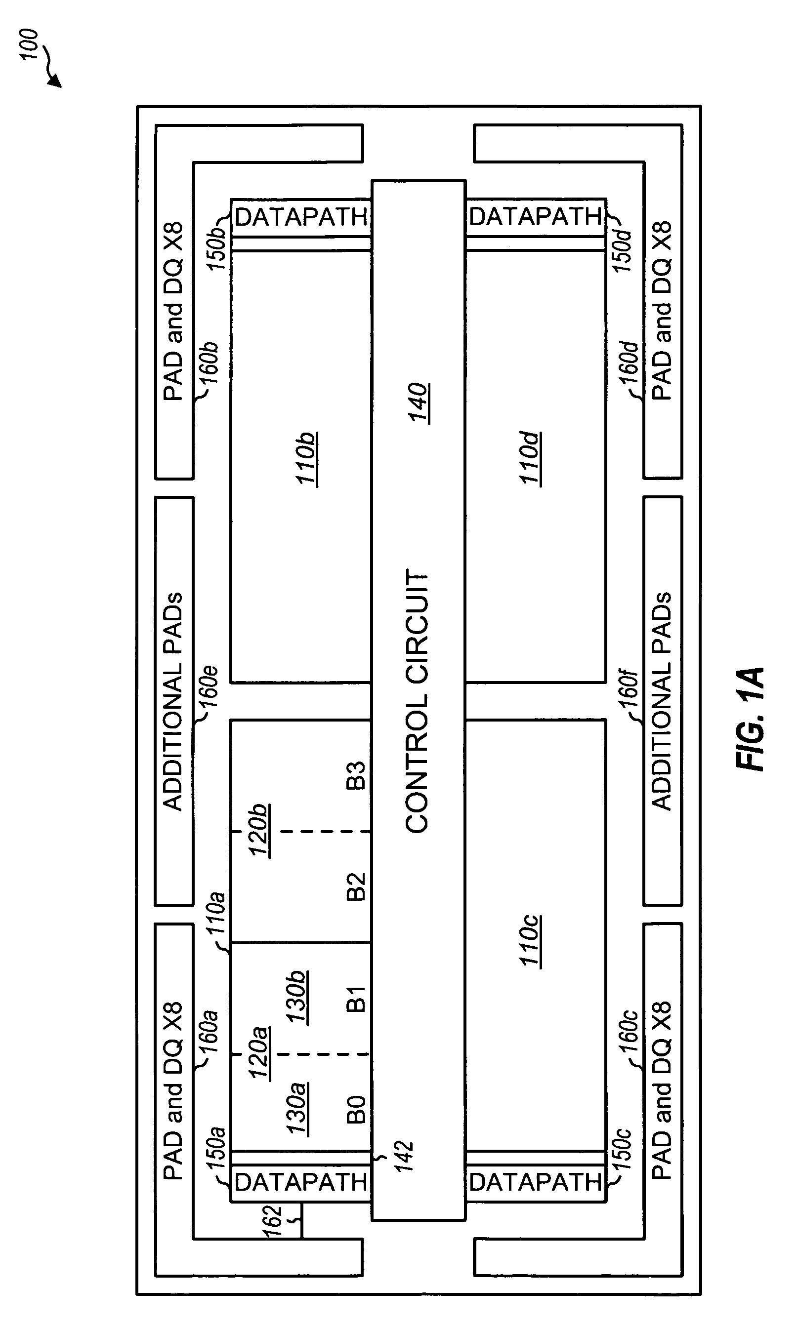
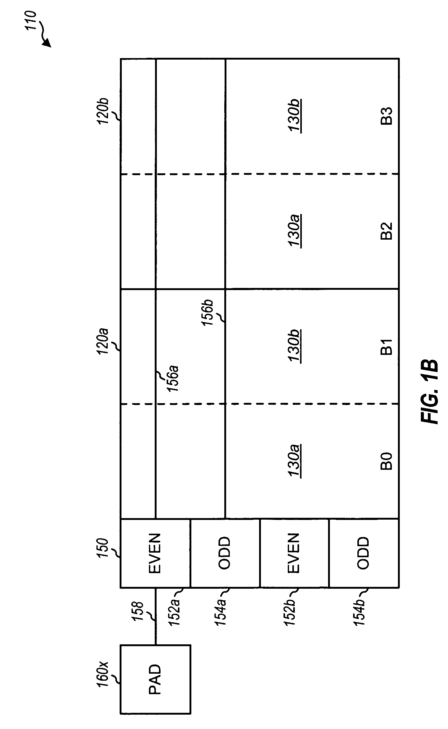
[0033]FIG. 1A is a diagram of a specific embodiment of a memory device 100. In this embodiment, memory device 100 includes four memory arrays 110a through 110d, with each memory array 110 including two memory banks 120a and 120b. Each memory bank 120 includes an upper half 130a and a lower half 130b. A control circuit 140 couples to memory arrays 110a through 110d and provides the necessary control signals, clock signals, and reference voltages. Additional control and support circuitry may be dispersed t...


PUM


Abstract

Data input and output circuits that support multi data rate and a number of timing schemes. In one design, a data output circuit includes an input multiplexer, data latches, an output multiplexer, and at least one output driver. The input multiplexer receives a set of data bits in a first order (e.g., odd and even) and provides the data bits in a second order (e.g., first and second). The data latches can latch the data bits with (1) a latch signal to satisfy memory access timing requirements and (2) a data write clock signal to satisfy output timing requirements. The output multiplexer multiplexes the latched data bits to provide time multiplexed data bits. The output driver(s) provide signal drive for the time multiplexed data bits. Clock signals with various timing characteristics can be used to allow the data output circuit to satisfy various timing requirements.

Description

BACKGROUND OF THE INVENTION[0001]The present invention relates generally to memory devices, and more particularly to data input and output circuits capable of supporting multi (e.g., double) data rate operation and a number of timing schemes.[0002]Memory devices are integral to computer systems, and to many electronic circuits. Continuous improvements in the operating speed and computing power of central processing units (CPUs) enable operation of an ever-greater variety of applications, many of which require larger and faster memories. Larger memories are characterized by having more memory cells to store more bits of data. Faster memories can be provided by reducing the time necessary for each read and write cycle and by allowing for access of multiple data bits on each clock cycle.[0003]Memory devices can be designed to support a number of operating modes such as a single data rate (SDR) and a double data rate (DDR) mode. In the SDR mode, one data bit is accessed (i.e., written t...

Claims


Application Information

Patent Timeline
IPC IPC(8): H04L12/50G11C8/00H04Q11/00
CPCG11C7/1051G11C7/106G11C7/1066G11C7/1078G11C7/1093G11C7/1087H04Q2213/13292H04Q2213/13103H04Q2213/13106
Inventor ZHENG, HUA
Owner WINBOND SYST LAB
Features
  • Generate Ideas
  • Intellectual Property
  • Life Sciences
  • Materials
  • Tech Scout
  • Unparalleled Data Quality
  • Higher Quality Content
  • 60% Fewer Hallucinations
Learn More