LED chip with integrated fast switching diode for ESD protection

a technology of esd protection and led chips, applied in the direction of basic electric elements, electrical equipment, semiconductor devices, etc., can solve the problems of reducing the area and light output of the light producing diode, inconsequential light output, and particularly susceptible to damage of leds, so as to reduce the series resistance of the esd diode, expand the chip virtually, and reduce the series resistance

Active Publication Date: 2006-06-20
JANSSEN PHARMA NV +1
View PDF8 Cites 146 Cited by
  • Summary
  • Abstract
  • Description
  • Claims
  • Application Information

AI Technical Summary

Benefits of technology

[0008]To reduce the series resistance of the ESD diode, the contact area between the metal layer and the exposed N-type material is made long and expands virtually the width of the chip. Various configurations of the PN junction and the N and P metal contacts for the ESD diode are described for reducing the series resistance and increasing the breakdown voltage.

Problems solved by technology

LEDs, especially gallium nitride-based LEDs, are particularly susceptible to damage with a reverse bias voltage across its anode and cathode.
One drawback associated with placing an ESD diode on the same chip as an LED intended to emit light is that the ESD diode uses up area on the chip, thus reducing the area and the light output of the light producing diode.
Although the ESD diode may output light when forward biased, such light output is inconsequential to its ESD function.
Another problem is that the high currents through the forward biased ESD diode must be carried through the series resistance of the diode.
Additionally, the structures of FIGS. 1–3 do not allow the light emitting diode and ESD diode to be individually tested for quality and reliability since the interconnections are already made on the chip.

Method used


Image

  • LED chip with integrated fast switching diode for ESD protection
  • LED chip with integrated fast switching diode for ESD protection
  • LED chip with integrated fast switching diode for ESD protection

Examples


Embodiment Construction

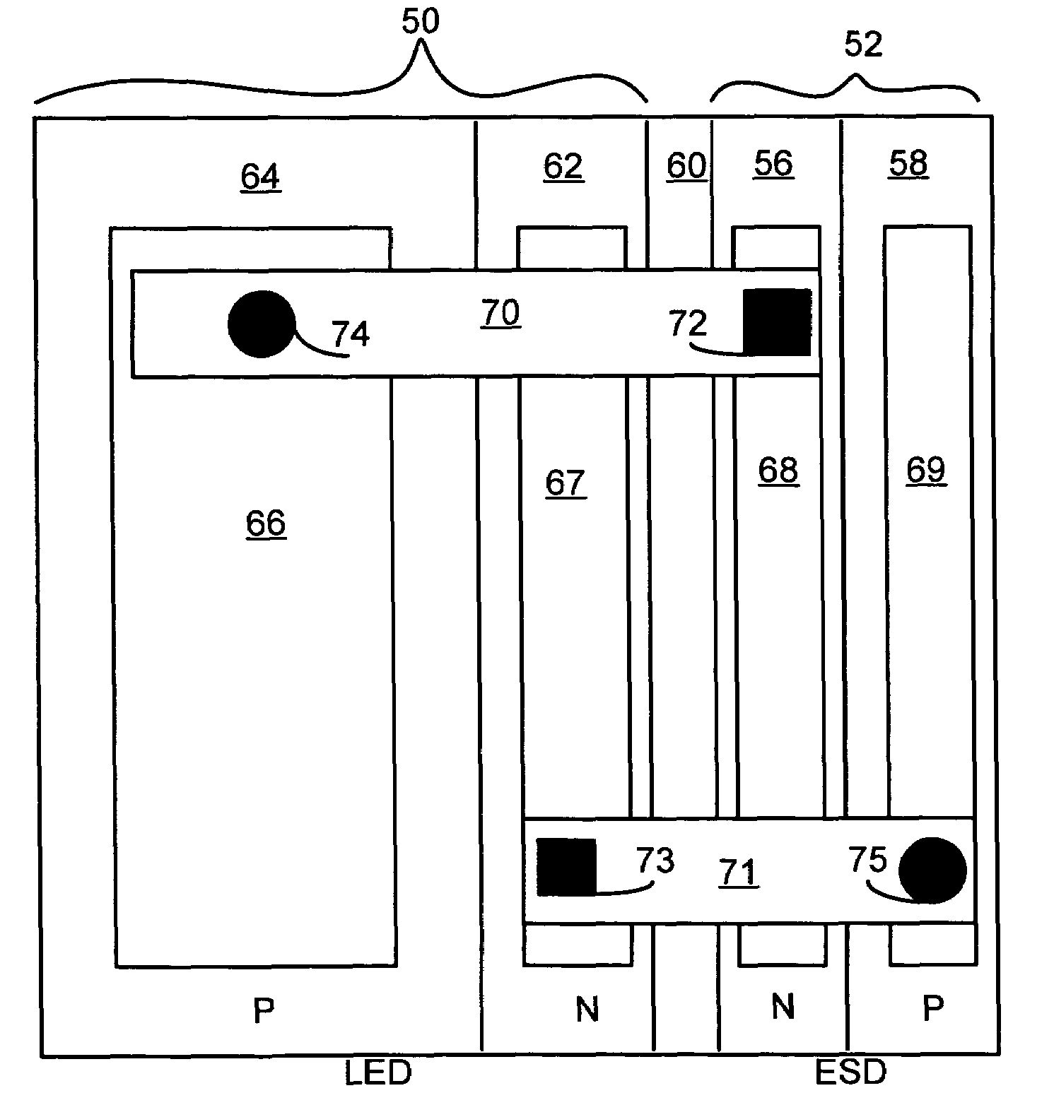
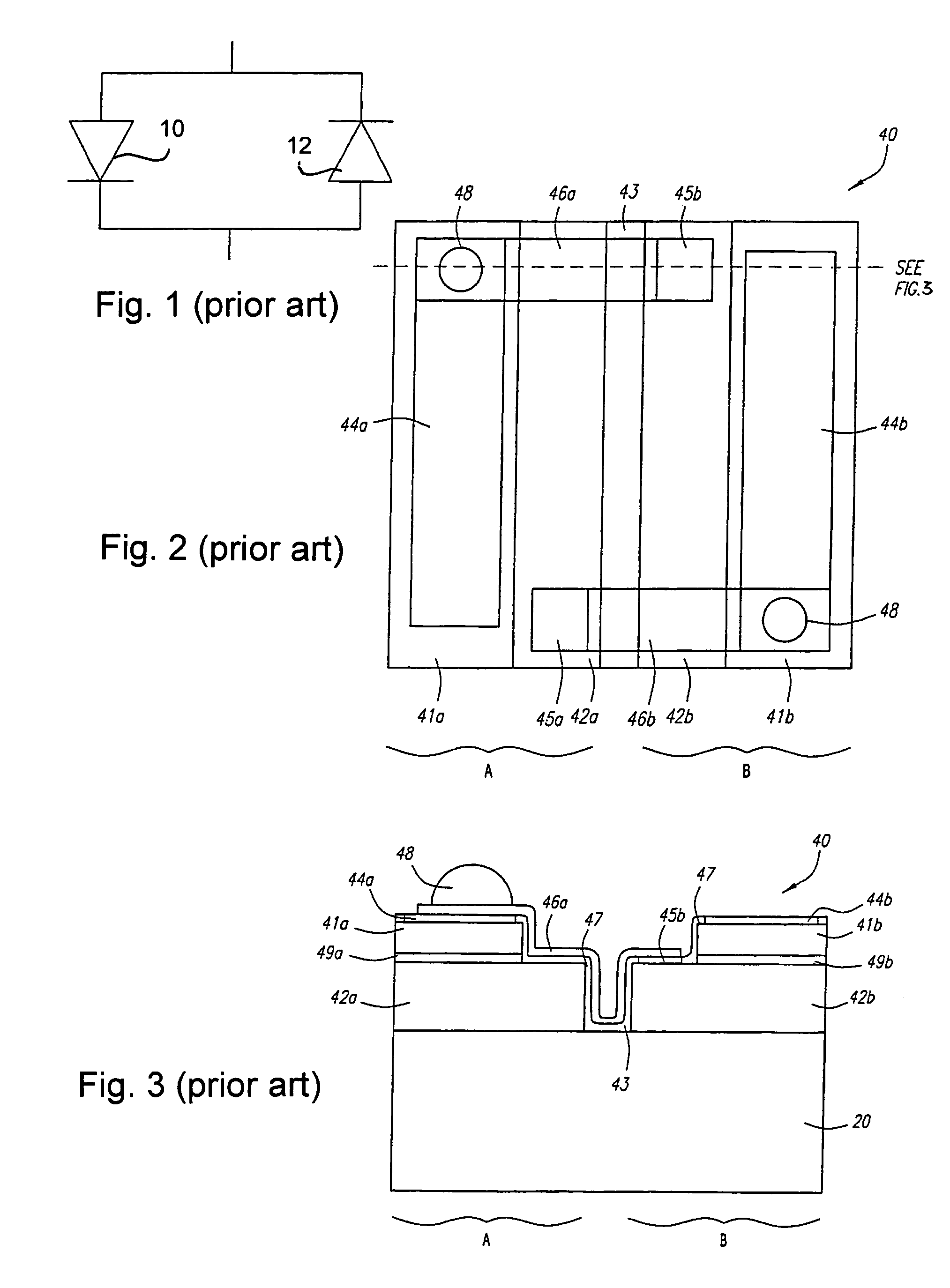
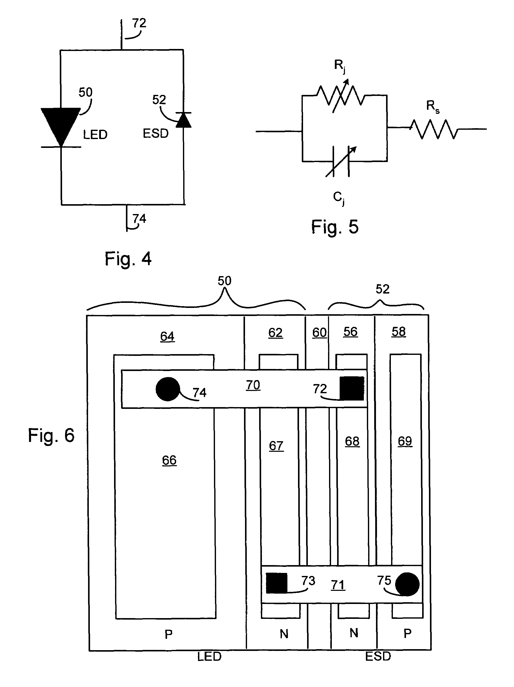
[0021]FIG. 4 is a schematic diagram similar to FIG. 1 except that the light emitting diode 50 is shown to be much larger than the ESD protection diode 52. Since diode 52 is not needed for its light output, its area may be very small. In one embodiment, the area of the ESD diode is less than 30 percent of the area of the chip. This allows more area of the chip to be utilized by the light emitting diode 50.

[0022]FIG. 5 illustrates the impedance components of the ESD diode 52. The impedance of the PN junction is largely determined by the junction resistance Rj and the junction capacitance Cj, where the impedance due to the capacitance is given by Z=1 / jωCj. This impedance remains largely invariant for a given junction area. However, the series resistance Rs of the diode is highly dependent upon the layout of the ESD diode 52. The series resistance becomes very significant during shunting of the high ESD current since a voltage is dropped across the series resistance equal to V=IRs. This...


PUM


Abstract

A relatively small ESD protection diode is formed on the same chip as a light emitting diode. In one embodiment, the ESD diode is a mesa-type diode isolated from the light emitting diode by a trench. To reduce the series resistance of the ESD diode, the PN junction and metal contact to the semiconductor material is made long and expands virtually the width of the chip. Various configurations of the PN junction and the N and P metal contacts for the ESD diode are described for increasing the breakdown voltage and for improved testing.

Description

FIELD OF THE INVENTION[0001]This invention relates to light emitting diodes (LEDs) and, in particular, to electrostatic discharge (ESD) protection for LED chips.BACKGROUND OF THE INVENTION[0002]Providing ESD protection for LED chips is well-known and commonplace. LEDs, especially gallium nitride-based LEDs, are particularly susceptible to damage with a reverse bias voltage across its anode and cathode. ESD voltages in normal environments can exceed 10,000 volts.[0003]One example of a way to provide ESD protection for an LED chip is illustrated in FIGS. 1–3, which are described in U.S. Pat. No. 6,547,249, issued to the present inventor and others. This patent is incorporated herein by reference. FIG. 1 illustrates two diodes formed on the same semiconductor chip connected in an anti-parallel configuration. LED 10 is forward biased in normal operation and emits light. Upon a reverse bias voltage being applied to the terminals of LED 10, the ESD protection diode 12 conducts so as to sh...

Claims


Application Information

Patent Timeline
Patent Type & Authority Patents(United States)
IPC IPC(8): H01L27/15H01L21/00H01L27/04H01L21/822H01L29/861
CPCH01L27/15H01L2224/16H01L2224/05548H01L2224/05573H01L2224/05624H01L2224/05639H01L2224/05666H01L2924/00014
Inventor BHAT, JEROME C.
Owner JANSSEN PHARMA NV
Why Eureka
Try Eureka