Optical subassembly

a sub-assembly and optical technology, applied in the field of optical circuits, can solve the problems of high frequency signal management, signal loss, cross talk, etc., and achieve the effect of reducing the number of components, reducing the number of parts, and improving the quality of the optical sub-assembly

Inactive Publication Date: 2006-06-27
INTEL CORP
View PDF13 Cites 37 Cited by
  • Summary
  • Abstract
  • Description
  • Claims
  • Application Information

AI Technical Summary

Problems solved by technology

One challenge to manufacturers of optical circuits such as transceivers that both transmit and receive signals and therefore may comprise VCSELs is the ability to bend or fold the light from a generally perpendicular or orthogonal transmission to a transmission lateral to the substrate and couplable to a fiber connection.
As circuits move from 2.5 to 10 gigabits per second, the concern of managing these high frequency signals, particularly concerns of cross talk, signal delays, and signal losses, increases.

Method used


Image

  • Optical subassembly
  • Optical subassembly
  • Optical subassembly

Examples


Embodiment Construction

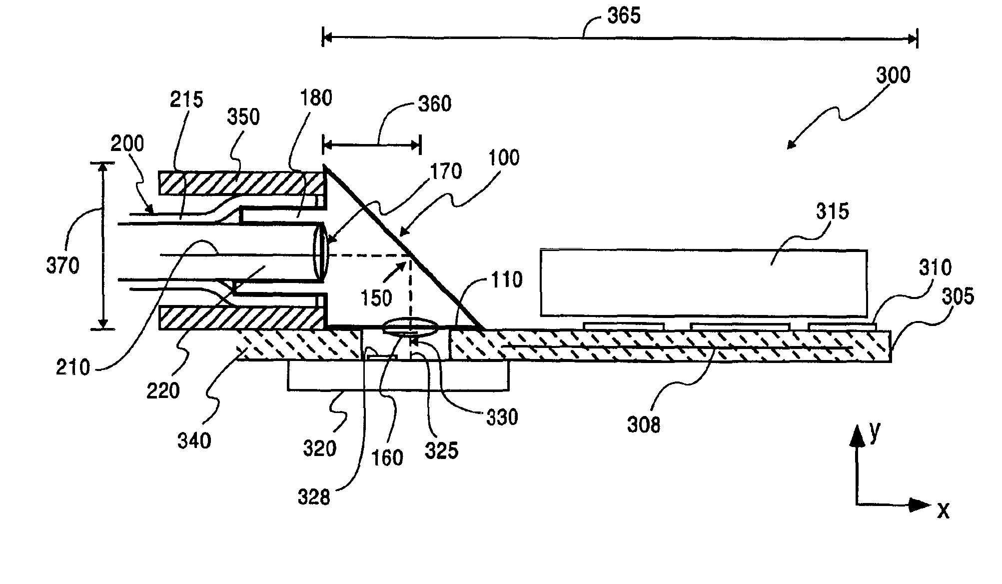
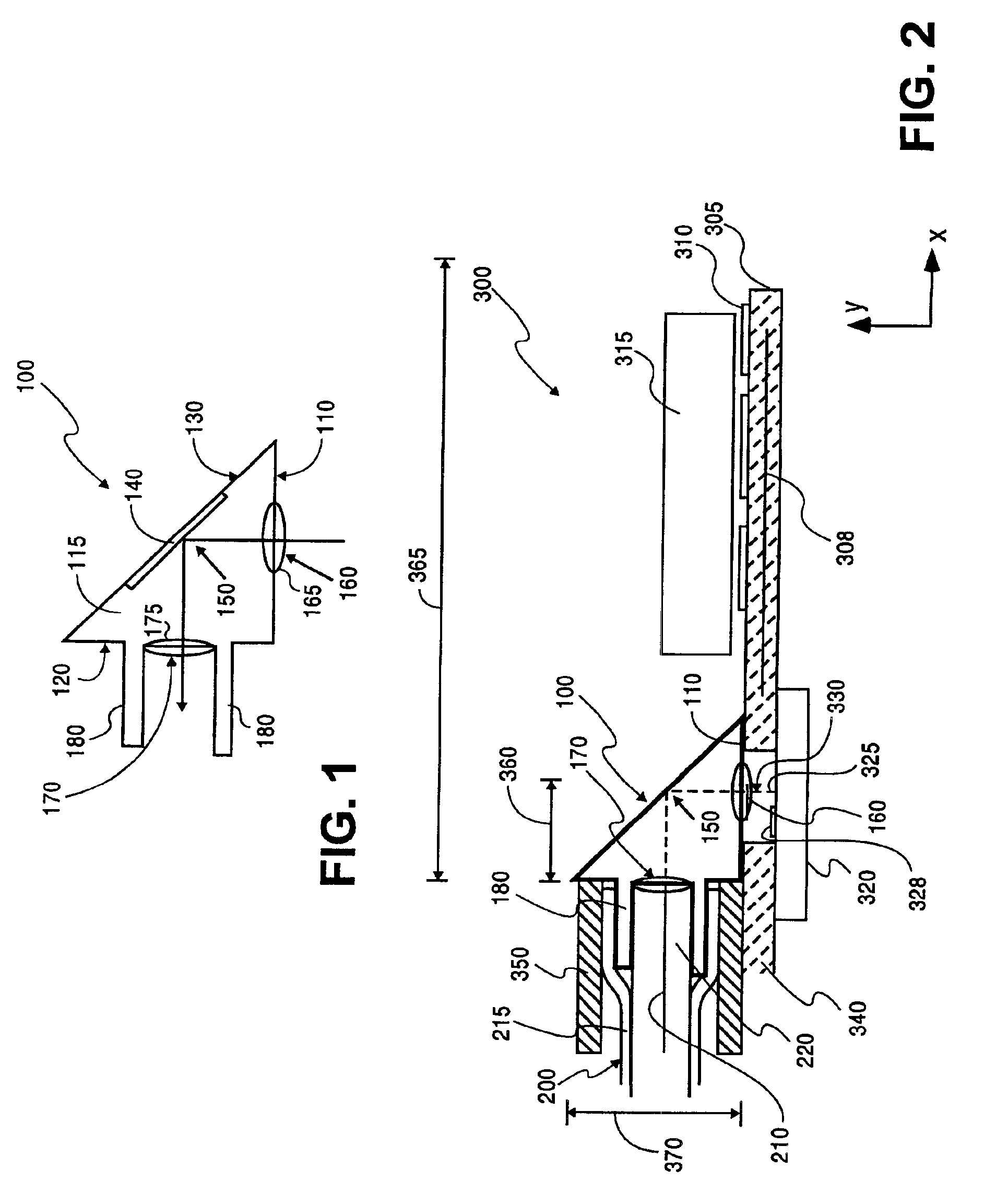
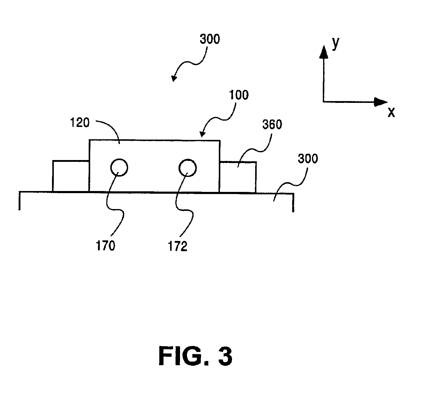
[0013]An apparatus is disclosed. In one embodiment, the apparatus is suitable as a subassembly of a transmitter, receiver, or transceiver of optical signals, particularly optical signals generated by semiconductor lasers such as VCSELs. In this regard, a system is also disclosed incorporating an apparatus as an optical subassembly of an optical circuit assembly. The optical assembly may be used to fold or bend emitted light from a VCSEL of a transceiver or a fiber to a photodetector to allow signal propagation in a desired plane. In this regard, the apparatus may be configured according to a desired formfactor for use within standard optical circuit (e.g., transceiver) packages. A technique for aligning a fiber to an optical circuit assembly is also disclosed.

[0014]FIG. 1 shows a cross-section of an embodiment of an apparatus that is suitable as a subassembly component for folding a light emission, such as a light emission from an optical transceiver. FIG. 1 shows subassembly 100 in...


PUM


Abstract

An apparatus including a base having a first opening of a dimension suitable to pass a light emission therethrough, a first side wall coupled to the base and having a second opening of a dimension suitable to pass a light emission therethrough, a second side wall coupled to the base and having a reflective component thereon, and the base, the first side wall, and the second side wall define an interior chamber with the reflective component disposed in the interior chamber; and a fiber connector extending from an exterior of the first side wall adjacent the second opening. A method including powering a laser disposed in a substrate coupling a fiber optic cable to an optical subassembly; and aligning the optical assembly over the transceiver board to capture the emitted light from the laser in the fiber optic cable.

Description

BACKGROUND OF THE INVENTION[0001]1. Field of the Invention[0002]The invention relates to optical circuits and more particularly to optical transceivers.[0003]2. Description of Related Art[0004]Optical circuits offer advantages over traditional electrical circuits, particularly, in their perceived ability to provide higher speed data transmissions. Such transmissions may take place not only between computers, but also within machines, in which case board-to-board and chip-to-chip data communication using optical circuits can be utilized.[0005]Semiconductor lasers typically come in two forms. A well known form is an “in-plane” laser, where the light inside the laser travels parallel to the substrate, such as a semiconductor substrate. More recently, a different laser geometry has developed, particularly for short distances (less than 100 meters) data communications, such as between computers. These lasers are typically known as “vertical cavity surface emitting lasers” (VCSELs). A VCS...

Claims


Application Information

Patent Timeline
Patent Type & Authority Patents(United States)
IPC IPC(8): G02B6/42G02B6/30
CPCG02B6/4214G02B6/4246G02B6/4292
Inventor MURALI, VENKATESANCRAFTS, DOUGLAS E.RAMALINGAM, SURESHZABORSKY, BRETT M.FLEISCHER, SIEGFRIED B.
Owner INTEL CORP
Why Eureka
Try Eureka