High density chalcogenide memory cells

a memory cell and high density technology, applied in the field of memory cell structure for semiconductors, can solve the problems of rams and roms having their own disadvantages, rams may loose data, and their memory contents may be compromised, so as to facilitate electrical isolation of memory cells

Inactive Publication Date: 2006-06-27
MACRONIX INT CO LTD
View PDF16 Cites 240 Cited by
  • Summary
  • Abstract
  • Description
  • Claims
  • Application Information

AI Technical Summary

Benefits of technology

[0013]The present invention relates to a particular arrangement of materials used to produce a chalcogenide alloy memory cell and a method for manufacturing the memory cell. Millions of these chalcogenide alloy memory cells may be created in a memory matrix to achieve one or more of the stated objectives. Each memory cell has a chalcogenide alloy structure having a side wall juxtaposed against a side wall of an electrode. This design permits a storage region within the chalcogenide alloy structure to be created in the area juxtaposed against the electrode. One of the advantages of the invention is that conventional integrated circuit processing techniques allow for very tight and repeatable control in manufacturing very thin electrodes. The precision manufacturing process of the electrodes allows for the creation of uniform storage regions within each memory cell across the entire memory matrix.
[0016]A contact may be created for each memory cell to provide a connection between the address rows and the electrodes. The contact may be comprised of a diode, connected in series with the contact, to thereby facilitate electrical isolation the memory cells from one other. Electrically isolating the memory cells insures that during an operation on a particular memory cell, the data contained within the remaining memory cells will not be corrupted by the operation.

Problems solved by technology

However, conventional RAMs and ROMs have their own disadvantages.
RAMs, while having fast data transfer rates and efficient writing architectures, must be continuously powered or their memory contents may be compromised.
Thus, RAMs may loose their data, i.e. they are volatile, when power is inadvertently or accidentally removed.
ROMs, while retaining their contents even in the absence of power, are limited in the number of times to which they may be written, the speed, and the manner in which they may be written.
Chalcogenide materials are also fast and consume very little electrical current.

Method used


Image

  • High density chalcogenide memory cells
  • High density chalcogenide memory cells
  • High density chalcogenide memory cells

Examples


Embodiment Construction

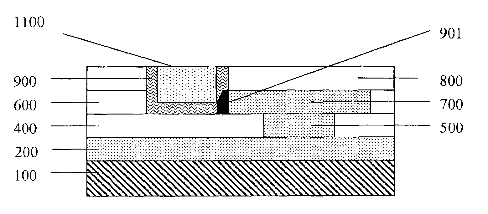
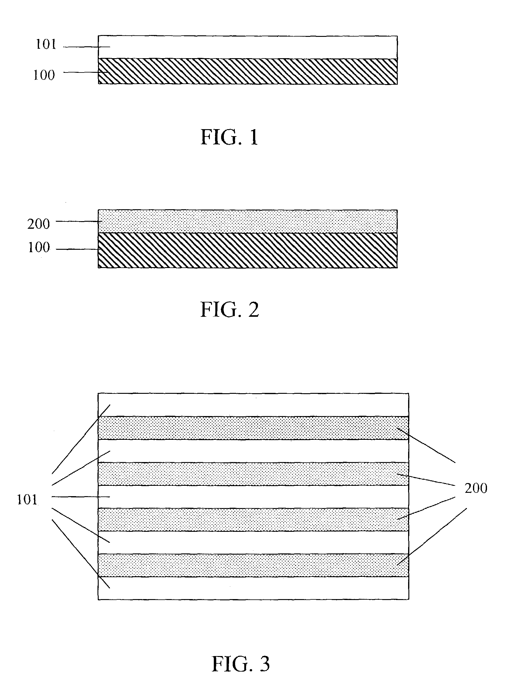
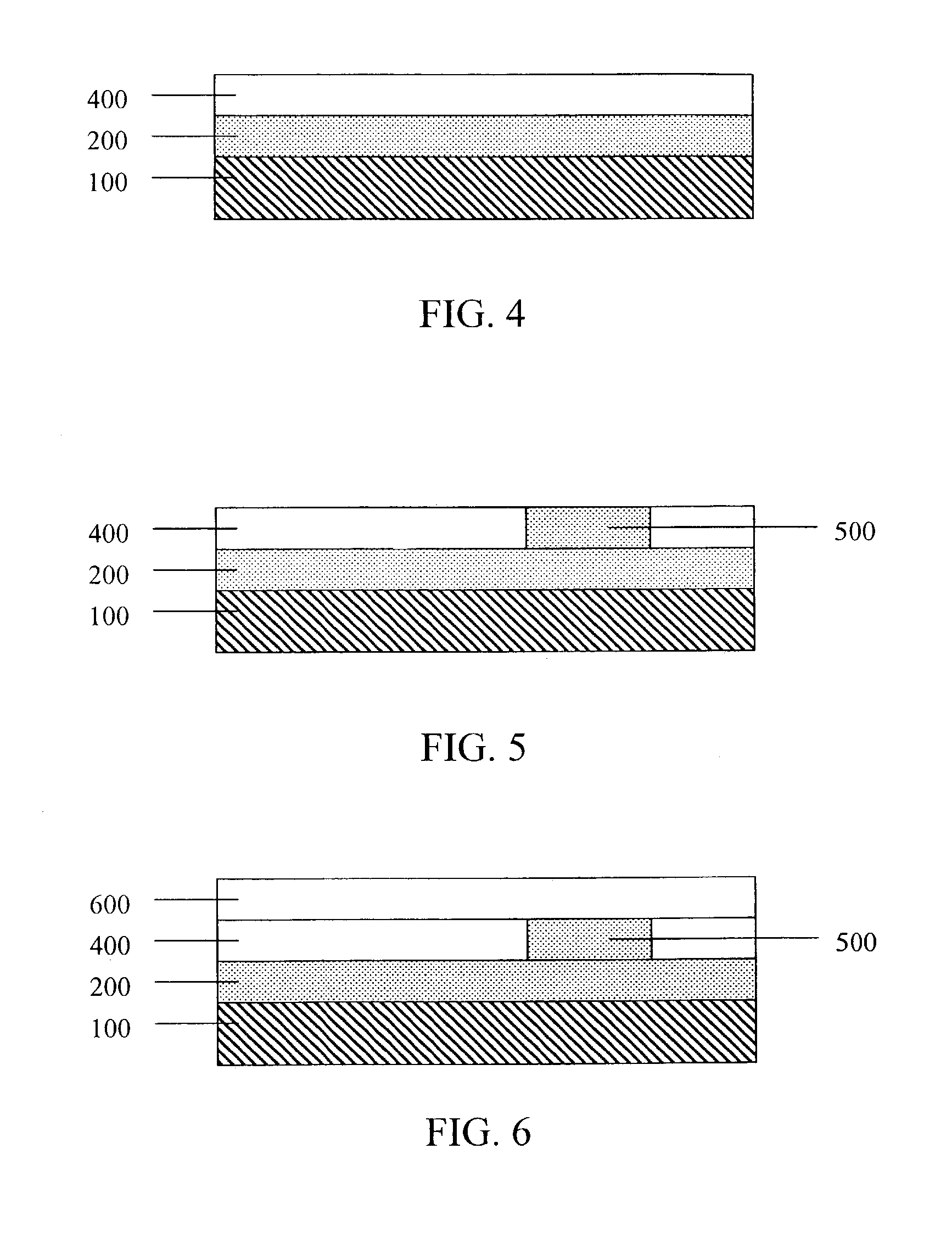
[0034]Reference will now be made in detail to the presently preferred embodiments of the invention, examples of which are illustrated in the accompanying drawings. Whenever possible, the same reference numbers are used in the drawings and the description to refer to the same or like parts. It should be noted that the drawings are in greatly simplified form and are not to precise scale. It should be noted that the drawings are in simplified form and are not to precise scale. In reference to the disclosure herein, for purposes of convenience and clarity only, directional terms, such as, top, bottom, left, right, up, down, over, above, below, beneath, rear, and front, are used with respect to the accompanying drawings. Such directional terms should not be construed to limit the scope of the invention in any manner. In the following description, numerous specific details are set forth illustrating Applicant's best mode for practicing the invention and enabling one of ordinary skill in t...


PUM

PropertyMeasurementUnit
thicknessaaaaaaaaaa
thicknessesaaaaaaaaaa

Abstract

A non-volatile memory cell is constructed from a chalcogenide alloy structure and an associated electrode side wall. The electrode is manufactured with a predetermined thickness and juxtaposed against a side wall of the chalcogenide alloy structure, wherein at least one of the side walls is substantially perpendicular to a planar surface of the substrate. The thickness of the electrode is used to control the size of the active region created within the chalcogenide alloy structure. Additional memory cells can be created along rows and columns to form a memory matrix. The individual memory cells are accessed through address lines and address circuitry created during the formation of the memory cells. A computer can thus read and write data to particular non-volatile memory cells within the memory matrix.

Description

BACKGROUND OF THE INVENTION[0001]1. Field of the Invention[0002]The present invention relates generally to a memory cell structure for semiconductors, and more particularly, to chalcogenide memory cells.[0003]2. Description of Related Art[0004]Integrated circuits, typically in the form of microprocessors, microcontrollers, or other logic circuits, are used to control the functions of many modern electronic devices. For example, integrated circuits are used to control the functions of computers, telephones, and many other consumer electronics. It is generally necessary for the integrated circuits to retrieve (read) and store (write) data as they perform their functions. The data may be in the form of instructions for the integrated circuits (e.g., a program), data necessary for the execution of a program, or data generated during the execution of the program. It is highly advantages to store the data in memory devices which are easily accessible by the integrated circuits.[0005]Many ...

Claims


Application Information

Patent Timeline
Patent Type & Authority Patents(United States)
IPC IPC(8): H01L27/108H01L27/24H01L45/00
CPCH01L45/06H01L45/1226H01L45/1273H01L27/2463H01L45/16H01L27/2409H01L45/144H10B63/20H10B63/80H10N70/823H10N70/8418H10N70/231H10N70/011H10N70/8828
Inventor LUNG, HSIANG LAN
Owner MACRONIX INT CO LTD
Why Eureka
Try Eureka