Double-depth shallow channel isolation groove and preparation method thereof

A technology of shallow trench isolation and isolation grooves, which is applied in radiation control devices, semiconductor/solid-state device manufacturing, electrical components, etc., can solve the problems of poor electrical performance of photosensitive devices and low electrical isolation performance of STI, and achieve improved performance , avoid double-slope morphology, and expand the effect of the process window

Active Publication Date: 2019-08-20
SHANGHAI INTEGRATED CIRCUIT RES & DEV CENT +1
View PDF21 Cites 10 Cited by
  • Summary
  • Abstract
  • Description
  • Claims
  • Application Information

AI Technical Summary

Problems solved by technology

[0004] However, in the traditional process of forming a double-depth STI structure, the performance of STI electrical isolation is low, and the electrical performance of the subsequently formed photosensitive device is poor.

Method used


Image

  • Double-depth shallow channel isolation groove and preparation method thereof
  • Double-depth shallow channel isolation groove and preparation method thereof
  • Double-depth shallow channel isolation groove and preparation method thereof

Examples


preparation example Construction

[0038] A traditional method for preparing a double-depth shallow trench isolation trench includes the following steps:

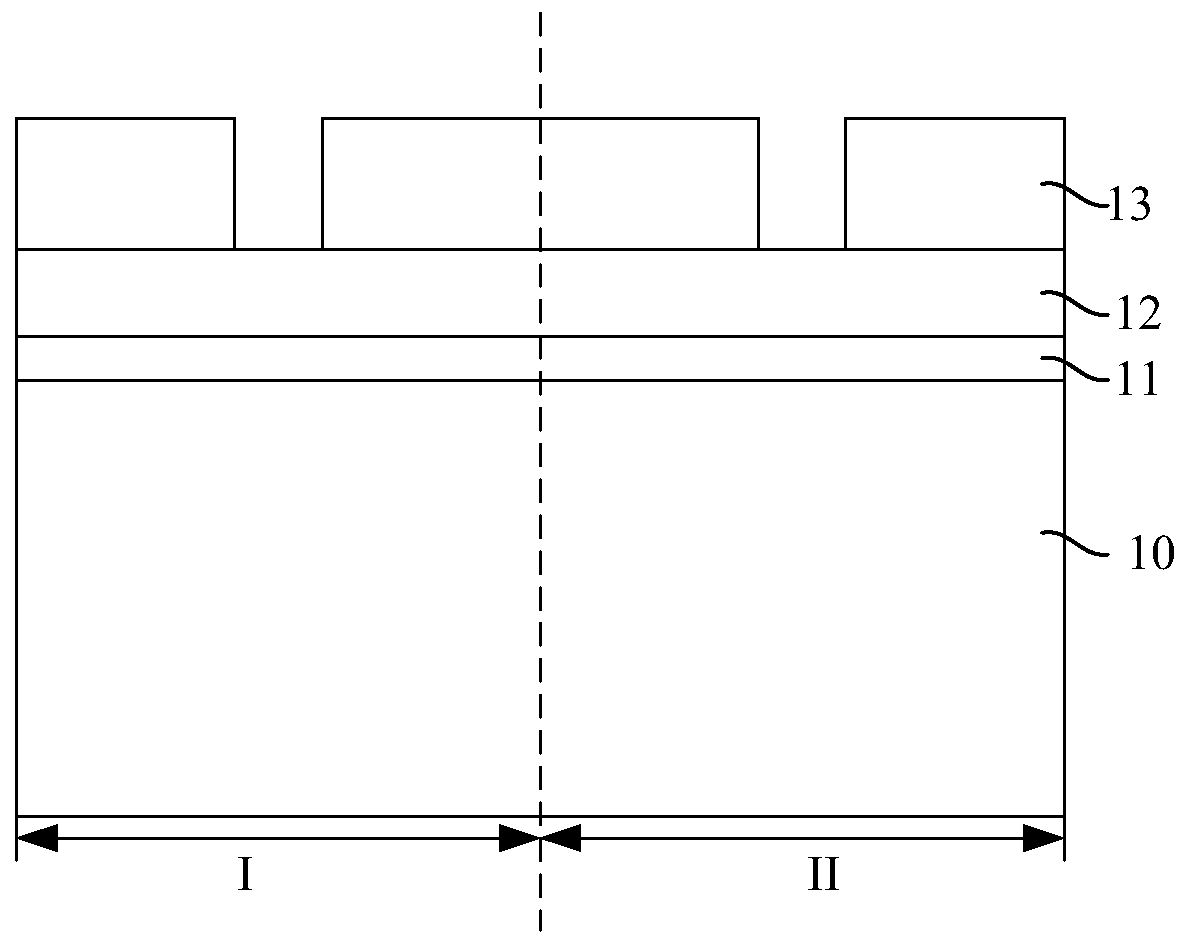
[0039] Step S11: See Figure 1a , providing a substrate 10 including a photosensitive region I and a logic region II, and sequentially depositing silicon oxide 11, a silicon nitride hard mask layer 12, and a patterned first photoresist 13 on the substrate 10;

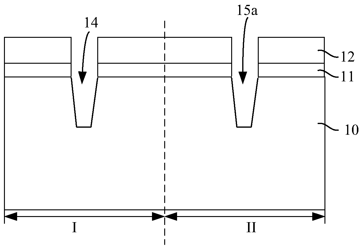
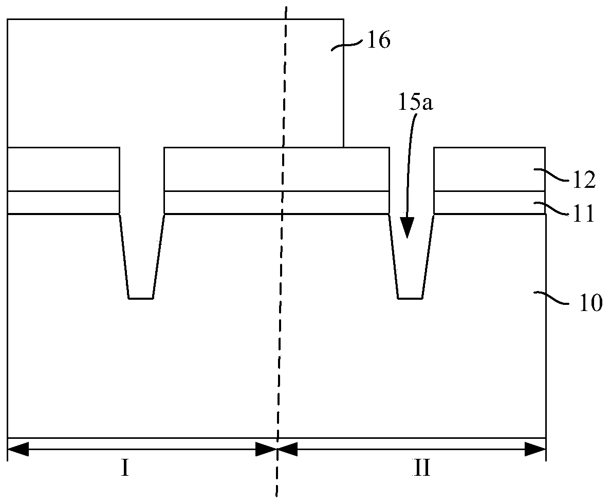
[0040] Step S12: See Figure 1b , the silicon nitride hard mask layer 12 and the silicon oxide 11 are sequentially etched by the first dry etching process, and the etching stops in the substrate 10 at a partial depth, so as to form the first isolation trench 14 and the second isolation trench 14. The first part 15a of the two isolation grooves, the first isolation groove 14 is located in the photosensitive area I, and the first part 15a is located in the logic area II, and the remaining first part 15a is cleaned and removed by an oxygen ashing method and a wet etching process. a photoresist 13;

[...


PUM


Abstract

The invention provides a double-depth shallow channel isolation groove and a preparation method thereof. The preparation method of the double-depth shallow channel isolation groove comprises the following steps: providing a substrate, and sequentially forming a hard mask layer and a graphical first photoresist layer on the substrate; taking the graphical first photoresist layer as a mask, etchingto form a first opening and a second opening, and then removing the first photoresist layer; forming a graphical second photoresist layer on the hard mask layer; taking the graphical second photoresist layer and hard mask layer as masks, etching to form a first part of a second isolation groove, and then removing the second photoresist layer; taking the hard mask layer as a mask, and etching to form the second part and the first isolation groove of the second isolation groove so that the first isolation groove of a photosensitive region and the second isolation groove of a logic region are formed at the same time. Thus, the electrical performance of the photosensitive device is improved, the STI electrical isolation performance is also improved, the process difficulty is reduced, and the process window is expanded.

Description

technical field [0001] The invention relates to the field of semiconductor manufacturing, in particular to a double-depth shallow trench isolation trench and a preparation method thereof. Background technique [0002] The shallow trench isolation (STI, Shallow Trench Isolation) process is one of the key processes in the formation of CMOS devices. As the device size continues to shrink, the thickness of the photoresist is limited, and the etching depth of STI is not greatly reduced. The photoresist cannot meet the thickness requirement of the STI etching mask layer, so after the 130nm technology node, the silicon nitride hard mask process is widely used in the prior art for STI etching. [0003] At the same time, CIS (CMOS Image Sensor, CMOS image sensor) products based on advanced technology platforms (<65nm) are currently hot spots in the field of chip manufacturing. Since the CIS chip has both a photosensitive area (Pixel) and a surrounding logic area (Logic), so that ...

Claims


Application Information

Patent Timeline
Patent Type & Authority Applications(China)
IPC IPC(8): H01L21/762H01L27/146
CPCH01L21/76224H01L27/1463H01L27/14687
Inventor 杨渝书伍强李艳丽
Owner SHANGHAI INTEGRATED CIRCUIT RES & DEV CENT
Why Eureka
Try Eureka