Closely-spaced VCSEL and photodetector for application requiring their independent operation

a laser and photodetector technology, applied in the field of vertical cavity surface emitting lasers and photodetectors, can solve the problems of low cost of data transmit and receive components, and low cost of fiber installation, so as to avoid other bipolar parasitic effects, reduce the cost of installation, and reduce the cost of operation

Inactive Publication Date: 2006-05-30
OPTICAL COMM PRODS
View PDF7 Cites 11 Cited by
  • Summary
  • Abstract
  • Description
  • Claims
  • Application Information

AI Technical Summary

Benefits of technology

[0022]Thus, in this preferred embodiment, a VCSEL circuit can be isolated from a p-i-n photodiode using a proton implant isolation region which is commonly used to isolate VCSELs formed in arrays. The anode contacts to the p region of the p-i-n photodiode may be coupled to ground so that the VCSEL structure which lies underneath the p-i-n photodiode is never turned on and other bipolar parasitic effects are avoided. The width of the proton implant isolation region is typically between 50 and 100 microns. Thus, the VCSEL and the p-i-n photodiode can be separated by an accurately known distance, significantly less than 25 microns if desired. Moreover, the difference in thickness between the VCSEL and the p-i-n photodiode is small, thereby permitting near-field coupling of the optoelectronic devices to fibers.
[0023]One significant advantage of the first embodiment of the invention is that it requires very few additional steps to an otherwise typical VCSEL manufacturing process. A second advantage is that, when an anti-reflection coating of silicon nitride is applied to the photo-receiving n region of the photodiode, in conjunction with the p-type mirror which underlies the p-i-n photodiode, a high degree of efficiency is achieved. The silicon nitride anti-reflection coating increases transmission of incoming light into the surface of the p-i-n photodiode. Additionally, any light which is not absorbed by the intrinsic layer of the photodiode on its way through will be reflected from the underlying p-type mirror back into the intrinsic layer and will then have a second opportunity to be absorbed.
[0024]A second preferred embodiment of the invention employs a VCSEL with an MSM photodiode. The VCSEL is manufactured on a semi-insulating substrate. Because the MSM photodetector employs the semi-insulating layer as its common cathode, the two optoelectronic devices are virtually isolated from one another electronically as a result. A photolithographically defined minimum spacing of 250 microns or less can also be achieved using the second preferred embodiment of the invention. An anti-reflection coating is also preferably employed over the MSM photodetector to increase efficiency. To further enhance electrical isolation between the two devices, an isolation region can also be formed, preferably by implantation. Another advantage of using an MSM photodiode is that the two anode terminals can be used to drive a differential amplifier, thereby permitting common-mode rejection of noise.

Problems solved by technology

For short-haul or “premises” applications, however, the cost of fiber and fiber installation is relatively less important than the cost of the many transmit and receive functions.
Thus, it is the cost of the data transmit and receive components, and particularly the optoelectronic devices and their packaging, that drives cost considerations for short-haul applications.
This is because the cost of complex beam-splitting components often cannot be justified.
The integration of the two devices into a single package is not, however, an easily achieved solution.
The prior art implementations as illustrated in FIGS. 1a–d and 2 cannot be readily adapted to multifiber ferrules currently available for unidirectional data transmission using VCSEL arrays.
Even if a substantially larger barrel could be created to integrate the light emitter and photodetector as commonly packaged to receive both a transmit and a receive fiber, it is not clear that the resulting package could provide the necessary separation of incoming and scattered outgoing light beams to prevent crosstalk between the transmit and receive signals (at least not without complex optics and possibly some form of isolation).
Closely spaced VCSELs and photodetectors can suffer leakage effects which can degrade the sensitivity of and induce excess noise into the operation of the photodetector.
Also, current leakage from the VCSEL to the photodetector can unacceptably alter the operating characteristics of the photodetector over time.
The use of GaAs receiver electronics, however, greatly adds to the cost of high speed data communications.

Method used


Image

  • Closely-spaced VCSEL and photodetector for application requiring their independent operation
  • Closely-spaced VCSEL and photodetector for application requiring their independent operation
  • Closely-spaced VCSEL and photodetector for application requiring their independent operation

Examples


Embodiment Construction

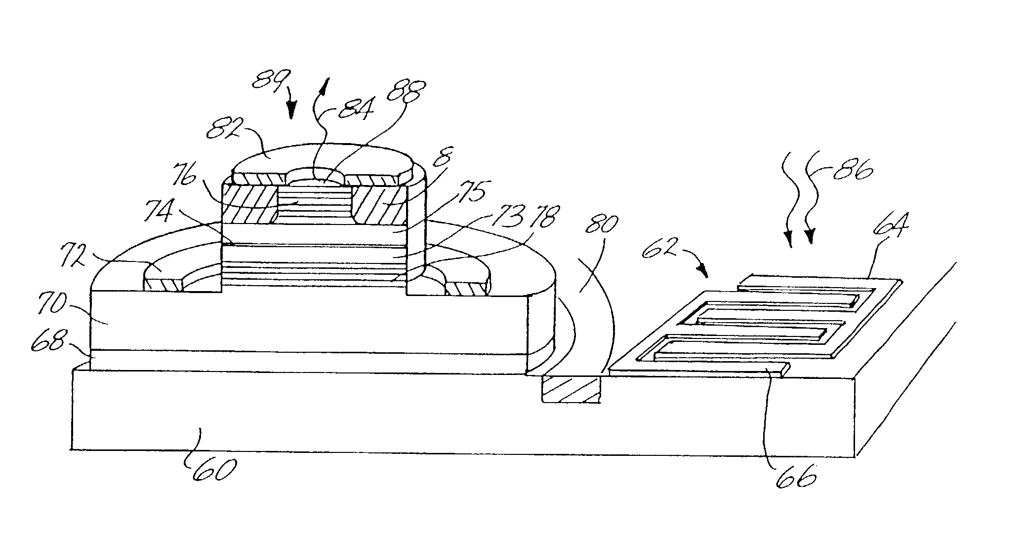
[0081]The present invention generally pertains to a monolithic semiconductor device having a VCSEL integrated with a photodetector on the same substrate, wherein the VCSEL and photodetector are to be operated independently as transmit and receive devices respectively. The VCSEL and photodetector are physically situated in close enough proximity to permit packaging of one or more pairs of the VCSEL and photodetector such that they may be coupled to multifiber ferrules having fiber spacing on the order of 250 microns or less. The present invention also includes a method of manufacturing the independently operated VCSEL and photodetector, as well as the packaging and coupling of one or more pairs of the integrated VCSEL and photodetector to multifiber ferrules.

[0082]A first preferred embodiment of the invention is now discussed in detail in conjunction with FIGS. 3 and 4. As shown in FIG. 3, a VCSEL and a metal-semiconductor-metal (MSM) photodetector are integrated on the same semi-ins...


PUM


Abstract

A monolithically integrated VCSEL and photodetector, and a method of manufacturing the same, are disclosed for applications where the VCSEL and photodetector require separate operation such as duplex serial data communications applications. A first embodiment integrates a VCSEL with an MSM photodetector on a semi-insulating substrate. A second embodiment builds layers of a p-i-n photodiode on top of layers forming a VCSEL using a standard VCSEL process. The p-i-n layers are etched away in areas where VCSELs are to be formed and left where photodetectors are to be formed. The VCSELs underlying the photodetectors are inoperable, and serve to recirculate photons which are not initially absorbed back into the photodetector. The transmit and receive pairs are packaged into a single package for interface to multifiber ferrules. The distance between the devices is precisely defined photolithographically, thereby making alignment easier. In a further alternate embodiment, a FET is coupled to the p-i-n photodiode to form an integrated detector preamplifier along with the VCSEL transmitter all on the same optical reference plane.

Description

CROSS-REFERENCE TO RELATED APPLICATIONS[0001]This application is a continuation of U.S. patent application Ser. No. 10 / 038,230, filed Jan. 3, 2002 now abandoned, which is a divisional of U.S. patent application Ser. No. 09 / 348,353 filed Jul. 7, 1999, now U.S. Pat. No. 6,392,256, which is a continuation-in part of U.S. patent application Ser. No. 08 / 803,891 filed Feb. 21, 1997, now U.S. Pat. No. 6,001,664, which is a continuation of U.S. patent application Ser. No. 08 / 593,117 filed Feb. 1, 1996, now abandoned, the contents of which are hereby incorporated by reference.FIELD OF THE INVENTION[0002]The present invention relates to vertical cavity surface emitting lasers (VCSELs) and photodetectors, and more particularly to the application of such optoelectronic devices where they must operate independently but where it is also desirable to have a transmitter and a receiver closely-spaced.BACKGROUND OF THE INVENTION[0003]There are a number of data communications applications that make us...

Claims


Application Information

Patent Timeline
Patent Type & Authority Patents(United States)
IPC IPC(8): H01L27/15H01L31/105H01L31/12H01S5/0232H01S5/026H01S5/042H01S5/183
CPCH01L31/105H01S5/0262H01L31/125H01S2301/176H01S5/02244H01S5/02248H01S5/02276H01S5/02284H01S5/0261H01S5/0264H01S5/06226H01S5/183H01S5/18308H01S5/18388H01S5/2063H01S5/02345H01S5/02325H01S5/02251H01S5/0232
Inventor SWIRHUN, STANLEY E.SCOTT, JEFFREY W.
Owner OPTICAL COMM PRODS
Why Eureka
Try Eureka