Micro-mechanism testing probe card based on electroplating technique and manufacturing method thereof

An electroplating process and micro-mechanical technology, applied in the direction of electronic circuit testing, process for producing decorative surface effects, metal material coating process, etc., can solve problems such as limiting the scope of application

Active Publication Date: 2010-01-20
深圳市道格特科技有限公司
View PDF5 Cites 1 Cited by
  • Summary
  • Abstract
  • Description
  • Claims
  • Application Information

AI Technical Summary

Problems solved by technology

However, due to the limitation of the design requirements of this silicon cantilever beam probe, in order to generate sufficient displacement of the needle tip, it is necessary to ensure a considerable length
This limits the probe array can only be densely arranged in one direction, which greatly limits its application range

Method used


Image

  • Micro-mechanism testing probe card based on electroplating technique and manufacturing method thereof
  • Micro-mechanism testing probe card based on electroplating technique and manufacturing method thereof
  • Micro-mechanism testing probe card based on electroplating technique and manufacturing method thereof

Examples


Embodiment 1

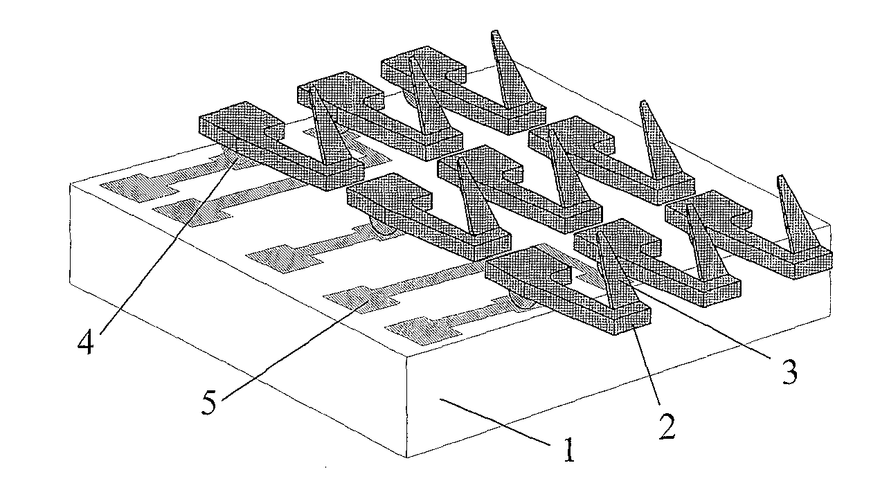
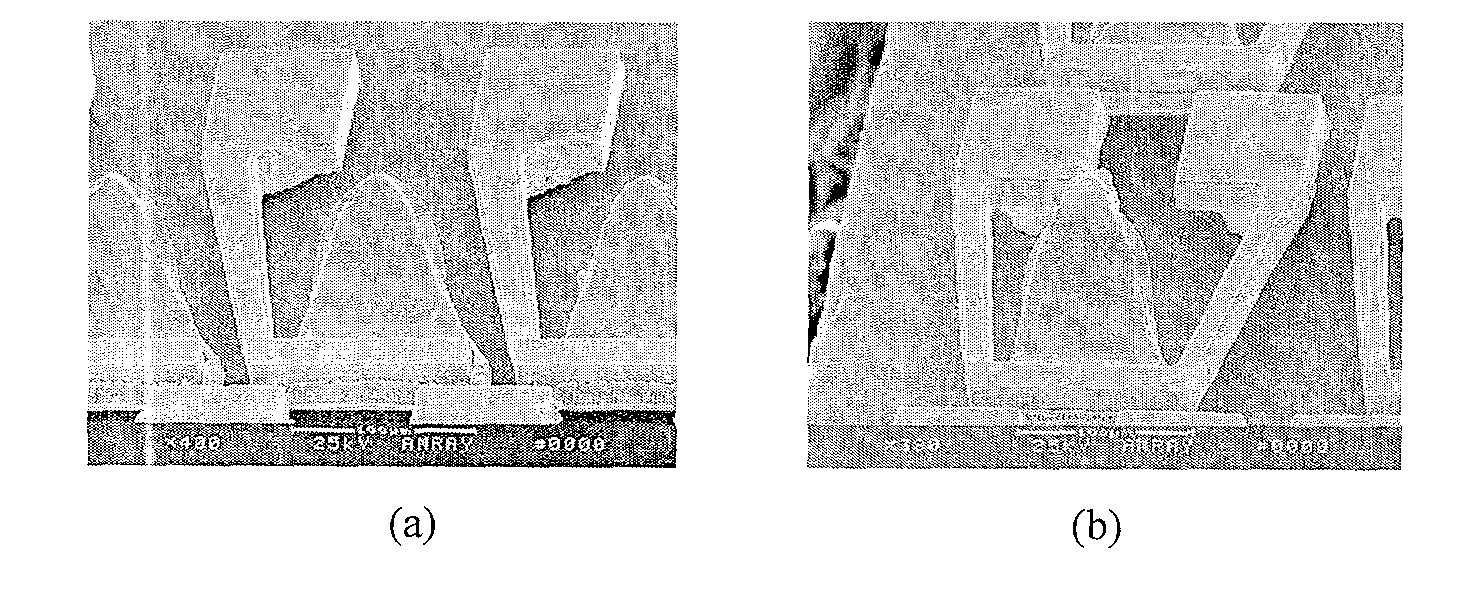
[0043] a Deposit or oxidize a layer of 0.5-2.5 μm oxide layer on the (100) silicon wafer, and then sputter or evaporate a layer of 0.1-0.5 μm titanium-copper metal seed layer on the oxide layer (as attached Figure 4 -a shown);

[0044] bUse a layer of 25-35μm thick photoresist for photolithography to form a pattern mask for the first electroplating (as attached Figure 4 -b shown);

[0045] c Carry out the first nickel electroplating, make the upper planar cantilever structure, remove the photoresist and metal seed layer; then, use glue spray photoetching to get the oxide layer pattern, in order to carry out the subsequent corrosion (as attached Figure 4 -c shown);

[0046] dUsing the oxide layer as a mask, use 50 °C, 40% potassium hydroxide solution (KOH) to perform anisotropic etching of silicon; and deposit a second time on the upper surface of the entire silicon wafer and the etched deep groove slope and bottom surface 0.1~0.5μm Ti-Cu metal seed layer (if attached F...


PUM

PropertyMeasurementUnit
sintering temperatureaaaaaaaaaa
thicknessaaaaaaaaaa
thicknessaaaaaaaaaa

Abstract

The invention relates to a micro mechanical testing probe card based on electroplating process and a manufacturing method thereof, and is characterized in that, cantilevers and probe tips are manufactured and formed on a silicon wafer with electroplated metal nickel; the probe tips are manufactured on an (111) inclined surface of the silicon wafer, and each probe tip is connected with a ceramic substrate with one or two probe cantilevers; the probe cantilevers and the probe tips adopt an isostress beam structure; probes on an flip chip substrate are intensively arranged in two directions. The manufacturing is characterized in that: firstly, the upper surface of the (100) silicon wafer is taken as the electroplated working face, and the probe cantilevers of a low stress nickel layer is formed by electroplating; and then a deep groove (111) inclined surface produced by anisotropic etching is taken as the working face, and the probe tips of the low stress nickel layer is formed by electroplating, and then the probes are connected with a package substrate by a flip chip process, and finally the probe structure is released through a method of removing the corrosion of the silicon wafer.

Description

technical field [0001] The invention relates to a wafer-level chip test probe based on a micro-mechanical method and a manufacturing method thereof, in particular to a micro-mechanical chip test probe based on an electroplating process and a manufacturing method thereof, belonging to the field of micro-electromechanical systems. Background technique [0002] In recent years, with the continuous progress of microelectronics technology, the integrated circuit manufacturing industry has developed rapidly. The production process of integrated circuit chips mainly includes front-end processing technology and back-end packaging and testing technology. Among them, the back-end packaging and testing process has already accounted for most of the cost of the entire production process. Therefore, adding wafer-level chip testing between the front-end processing technology and the back-end packaging and testing technology has become a necessary means to reduce chip costs. Probe cards a...

Claims


Application Information

Patent Timeline
Patent Type & Authority Patents(China)
IPC IPC(8): B81B3/00B81C1/00G01R1/073G01R31/28
Inventor 李昕欣汪飞封松林
Owner 深圳市道格特科技有限公司
Why Eureka
Try Eureka