Semiconductor structure

A technology of semiconductor and ring structure, which is applied in the direction of semiconductor devices, electrical components, circuits, etc., can solve problems such as the difficulty of reducing parasitic effects, achieve the effects of reducing parasitic effects, increasing equivalent parasitic resistance, and improving component performance

Active Publication Date: 2018-01-30
RICHWAVE TECH CORP
View PDF5 Cites 1 Cited by
  • Summary
  • Abstract
  • Description
  • Claims
  • Application Information

AI Technical Summary

Problems solved by technology

However, when used in higher frequency operations, such as radio frequency (radiofrequency) applications, the parasitic effects are still difficult to reduce, so a solution is needed in the art to reduce the parasitic effects of transistor components more effectively

Method used


Image

  • Semiconductor structure
  • Semiconductor structure
  • Semiconductor structure

Examples


Embodiment Construction

[0044] Specific embodiments of the present invention will be described in detail below in conjunction with the accompanying drawings. However, the present invention should be understood as not limited to such embodiments described below, and the technical idea of ​​the present invention can be implemented in combination with other known technologies or other technologies having the same functions as those known technologies.

[0045] In the description of the following specific embodiments, in order to clearly demonstrate the structure and working mode of the present invention, many directional words will be used to describe, but "front", "rear", "left", "right", "outer Words such as ", "inwardly", "outwardly", "inwardly", "axially" and "radially" are to be understood as convenient terms and should not be understood as limiting terms.

[0046] Attached below Figure 1-19 Specific embodiments of the present invention will be described in detail.

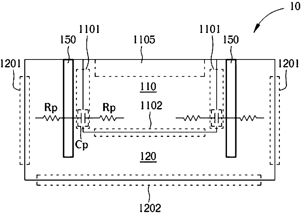
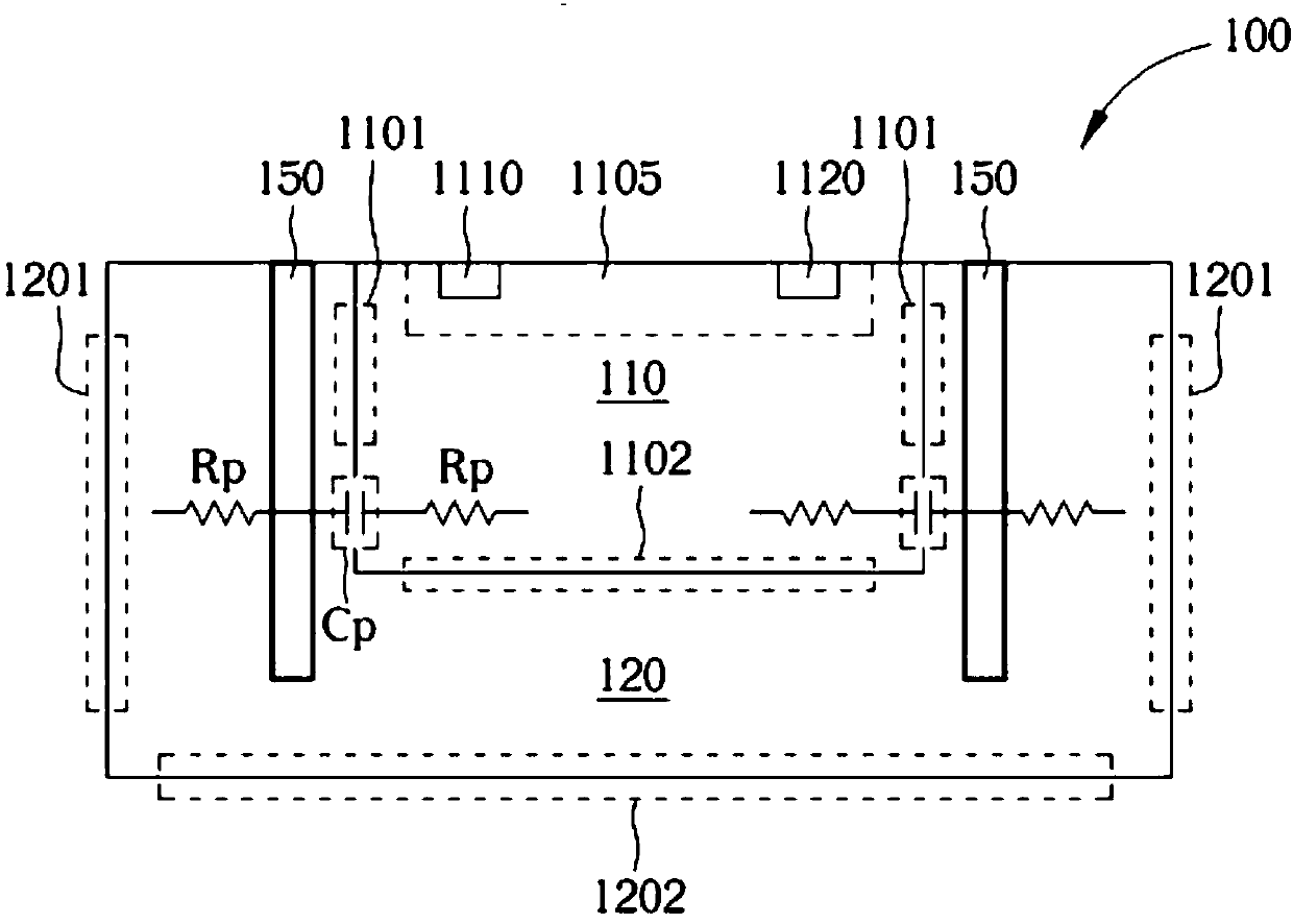
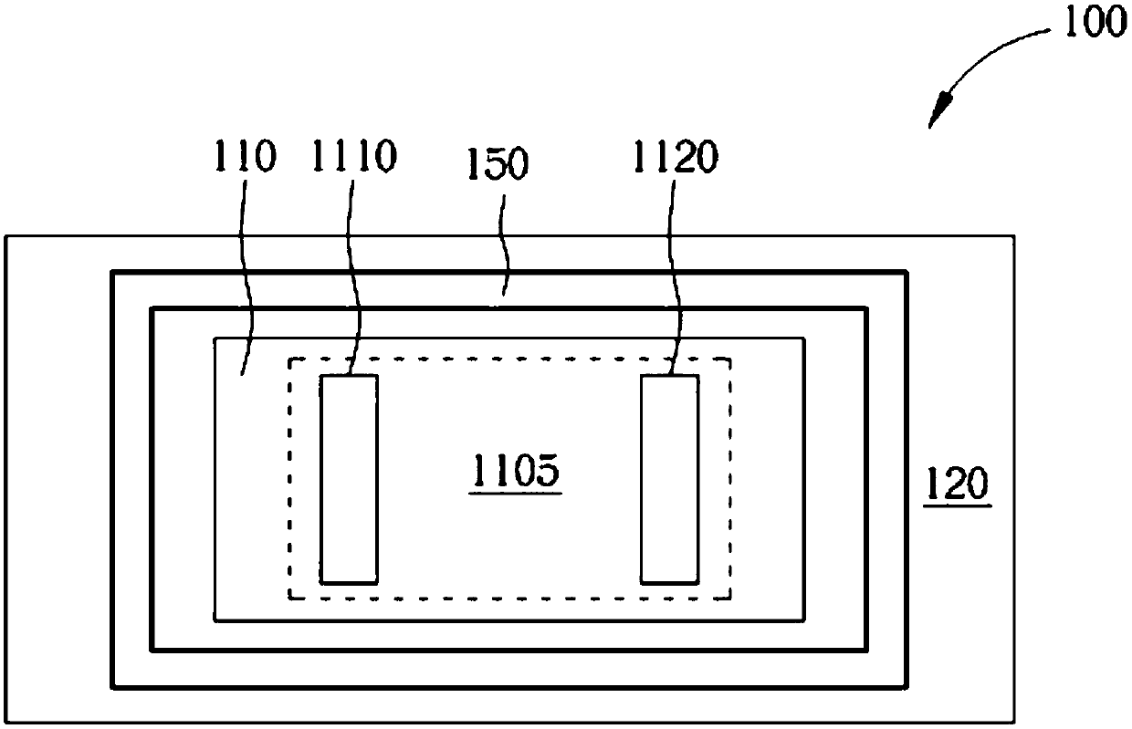
[0047] figure 1 is a schema...


PUM


Abstract

The invention discloses a semiconductor structure. The structure comprises a first well area, a semiconductor component, a second well area and a first separating layer, wherein the semiconductor component forms on or is contacted with the first well area; the first well area forms on the second well area; and the first separating layer is used for reducing a parasitic effect of the first well area and the second well area. A depth of a bottom of the first separating layer at least reaches a depth of a bottom of the first well area. The first separating layer is an annular structure which is formed along a lateral boundary of the first well area. A mixed type of the second well area is different from a mixed type of the first well area.

Description

technical field [0001] The present invention relates to a semiconductor structure, especially a semiconductor structure with an isolation layer to reduce parasitic effects. Background technique [0002] With the gradual popularization of high-frequency applications, the manufacturing process of semiconductor structures also faces the problem of parasitic effects caused by high-frequency operation, which increases parasitic capacitance and parasitic resistance. For example, in a general single-well CMOS device, there is only a single well region, which is disposed on a semiconductor substrate. When the single-well transistor structure operates at high frequency, The parasitic effect between the well area and the substrate will cause interference and lead to poor circuit characteristics. Therefore, there are multi-well semiconductor devices in the art, such as triple-well transistor devices, which use multi-well regions to provide higher isolation effect. However, when used ...

Claims


Application Information

Patent Timeline
Patent Type & Authority Applications(China)
IPC IPC(8): H01L29/06
Inventor 陈智圣林昭毅
Owner RICHWAVE TECH CORP
Why Eureka
Try Eureka