
A programmable non volatile memory unit, array and its making method

A memory cell, non-volatile technology, applied in the field of arrays and their manufacturing, programmable non-volatile memory cells, can solve the problems of reducing the reliability of logic devices and increasing costs, avoiding the effect of small size, reducing manufacturing Cost and power consumption, the effect of avoiding parasitics

Active Publication Date: 2010-02-10
GIGADEVICE SEMICON (BEIJING) INC
View PDF6 Cites 1 Cited by
  • Summary
  • Abstract
  • Description
  • Claims
  • Application Information

AI Technical Summary

Problems solved by technology

Therefore, the use of programmable non-volatile memory cells based on fuse or anti-fuse manufacturing technology not only increases the cost of SOC, but also greatly reduces the cost of logic devices due to the special process and special materials used in the manufacturing process. reliability

Method used


Image

  • A programmable non volatile memory unit, array and its making method
  • A programmable non volatile memory unit, array and its making method
  • A programmable non volatile memory unit, array and its making method

Examples


Embodiment Construction

[0064] Specific embodiments of the present invention will be described in detail below in conjunction with the accompanying drawings.

[0065] In the semiconductor logic manufacturing process, in order to improve the performance of integrated circuits, it is necessary to use refractory metal silicide (Salicide) to reduce the parasitic resistance of the active region and polysilicon. Finally, a layer of metal is deposited on the silicon surface and reacted with silicon to form a metal silicide; the remaining metal is removed after the reaction is completed. Since the metal does not react with the insulating layer, it does not affect the performance of the insulating layer.

[0066] In the self-aligned refractory metal silicide manufacturing process, most of the active area and polysilicon of the large-scale integrated circuit are covered by low-resistance metal silicide. However, some areas, such as high-resistance polysilicon and active areas that are prone to breakdown, requ...


PUM


Abstract

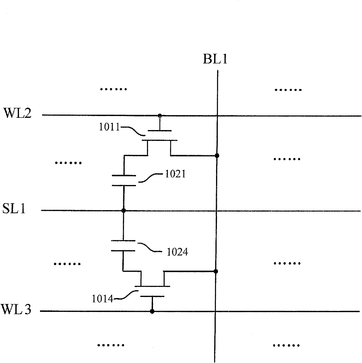
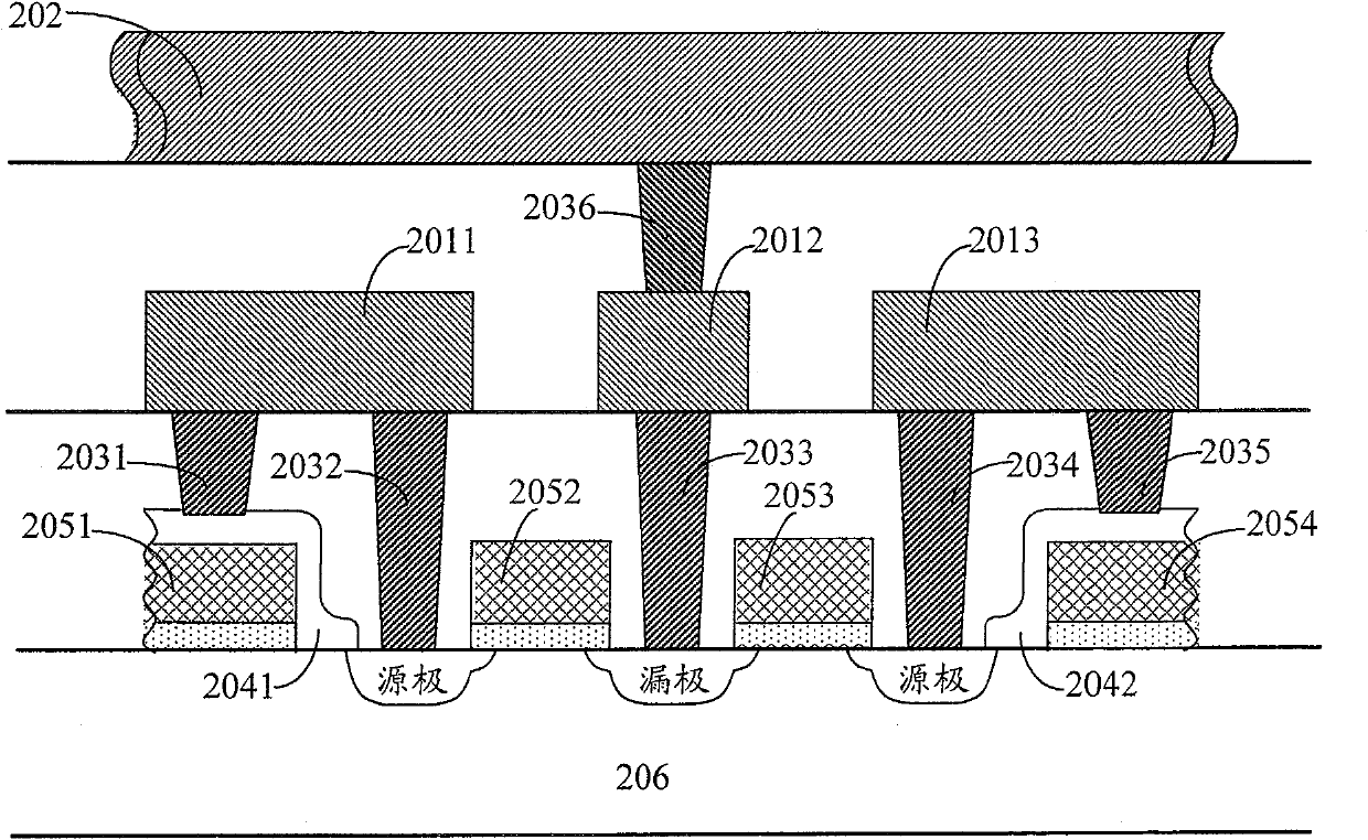
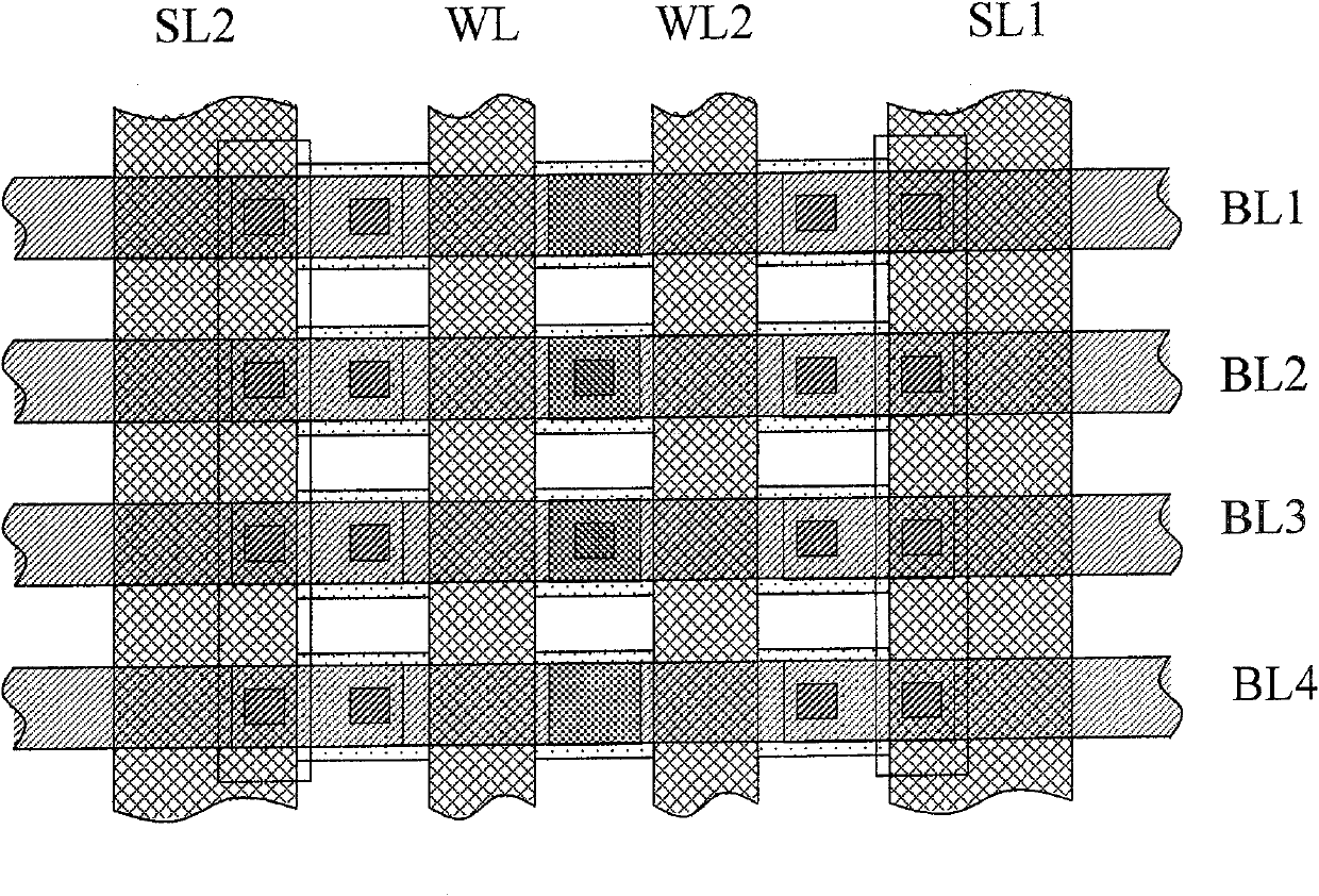
The invention discloses a programmable nonvolatile storage unit and an array, and the manufacturing method thereof. The device comprises a metal layer, a contact hole, a barrier layer, a plurality ofpolysilicons in the passive area, a plurality of polysilicons in the active area, and a substrate in the active area. A plurality of transistors are formed by the polysilicons in the active area and asubstrate in the active area; a plurality of source lines are formed by the polysilicons in the passive area; A plurality of word lines are formed by the polysilicons in the passive area. A pluralityof bit lines are formed by the metal lines in the metal layer. A capacitor is formed by connecting the metal layer, the connecting hole, the barrier layer, and the polisilicons in the passive area one by one. The storage unit is formed by means of corresponding series connection between the transistors and the capacitor and arrayed among the word-lines, the bit-lines and the source lines, which correspond to the storage unit. The invention improves the storage stability, decreases the area of the storage, and popularizes the application of VLSI.

Description

technical field [0001] The invention mainly relates to a semiconductor memory device, in particular to a programmable non-volatile memory unit, an array and a manufacturing method thereof. Background technique [0002] The manufacture of a System On Chip (SOC, System On Chip) is mainly based on a logic process, and designers often need to integrate a large number of non-volatile memory units inside the SOC during the R&D and design process of the SOC. According to the different uses of the designed SOC, the designer selects the appropriate type and function of the non-volatile storage unit as the internal storage unit of the SOC. [0003] Currently, nonvolatile storage units include read-only nonvolatile storage units, programmable read-only nonvolatile storage units, programmable erasable read-only nonvolatile storage units, and the like. Among them, the existing programmable non-volatile memory unit has the following deficiencies in its structure and design method: [00...

Claims


Application Information

Patent Timeline
Patent Type & Authority Patents(China)
IPC IPC(8): H01L27/115H01L23/522H01L21/8247H01L21/768H10B69/00
Inventor 朱一明胡洪
Owner GIGADEVICE SEMICON (BEIJING) INC
Learn More