Adjustable self-aligned air gap dielectric for low capacitance wiring

a dielectric and low capacitance technology, applied in the direction of semiconductor devices, semiconductor/solid-state device details, electrical apparatus, etc., can solve the problems of increasing increasing the difficulty of chip construction, and increasing the difficulty of chip operation, so as to reduce the width of copper lines, reduce the resistance of copper wiring, and reduce the capacitance

Active Publication Date: 2006-07-04
GLOBALFOUNDRIES U S INC
View PDF16 Cites 239 Cited by
  • Summary
  • Abstract
  • Description
  • Claims
  • Application Information

AI Technical Summary

Benefits of technology

[0007]It is another object of the present invention to provide a low capacitance dielectric that does not provide problems with porosity as copper line widths decrease in semiconductor circuits.
[0008]A further object of the invention is to provide a low capacitance dielectric that does not contribute to rise of copper resistivity as copper line widths decrease in semiconductor circuits.
[0009]It is yet another object of the present invention to provide a low capacitance dielectric that is compatible with conductor liner deposition processes.

Problems solved by technology

Because of continuing decreases in size of circuit components in semiconductor chips, there are a number of interconnect wiring challenges facing the technical community over the next few technology generations.
Among these challenges is the problem of undesirable capacitance in dielectric materials between circuit wiring.
However, because these materials generally have reduced mechanical strength and thermal conductivity, it is more difficult to build the chip and dissipate heat during chip operation.
Another challenge in the next few technology generations is presented by the expectation that the resistivity of copper wiring will begin to rise as the wire line width starts to approach its electron mean free path.
An additional challenge expected by the 65 nm line width generation is that physical vapor deposition (PVD), or sputtered, barriers will need to be replaced with chemical vapor deposition (CVD) or atomic layer deposition (ALD) barriers to meet ongoing thickness reductions and improved conformality requirements.
Also, depending upon the maximum pore size of the porous low k dielectric material, the thinner liners may not be able to provide continuous coverage to prevent copper diffusion into the adjacent dielectric material.

Method used


Image

  • Adjustable self-aligned air gap dielectric for low capacitance wiring
  • Adjustable self-aligned air gap dielectric for low capacitance wiring
  • Adjustable self-aligned air gap dielectric for low capacitance wiring

Examples


Embodiment Construction

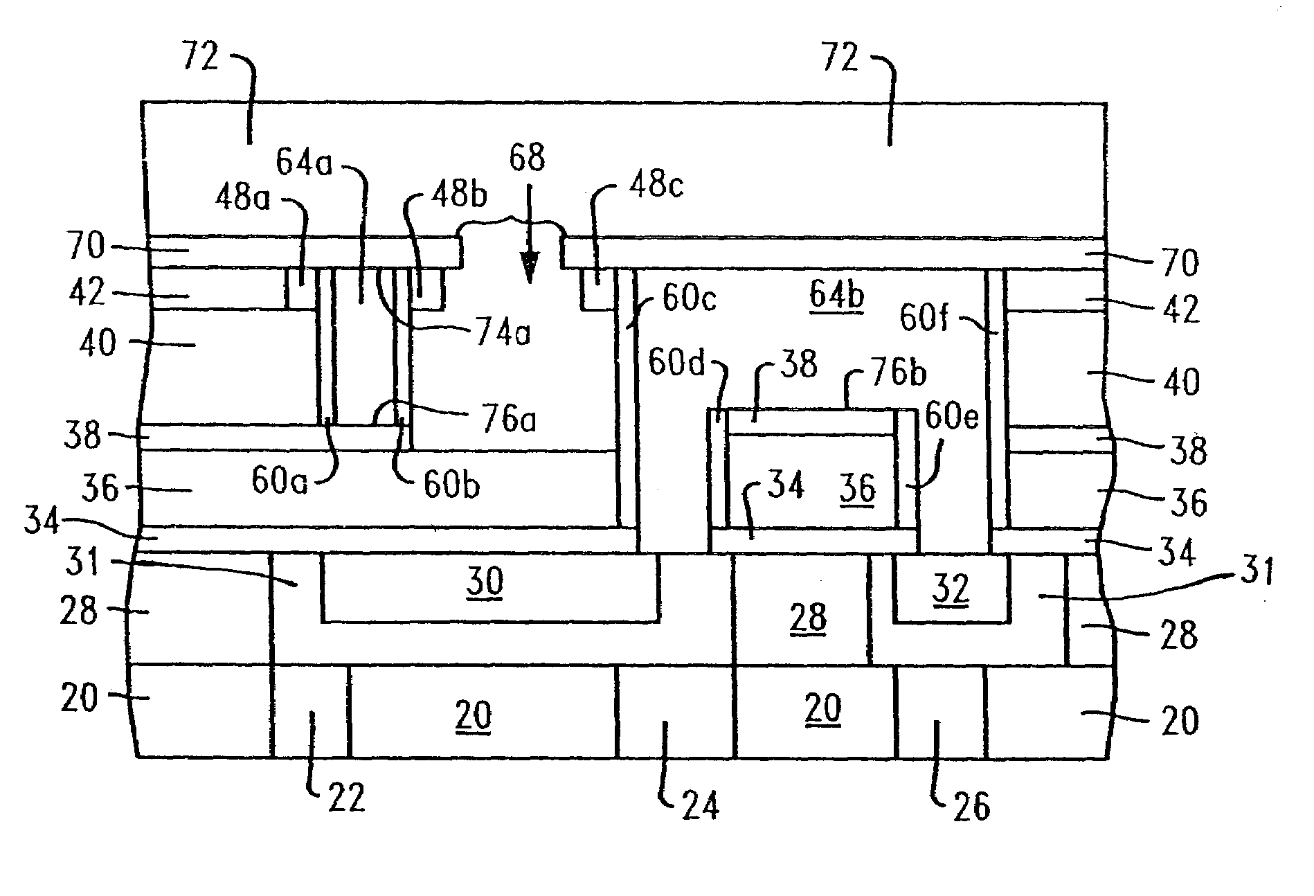
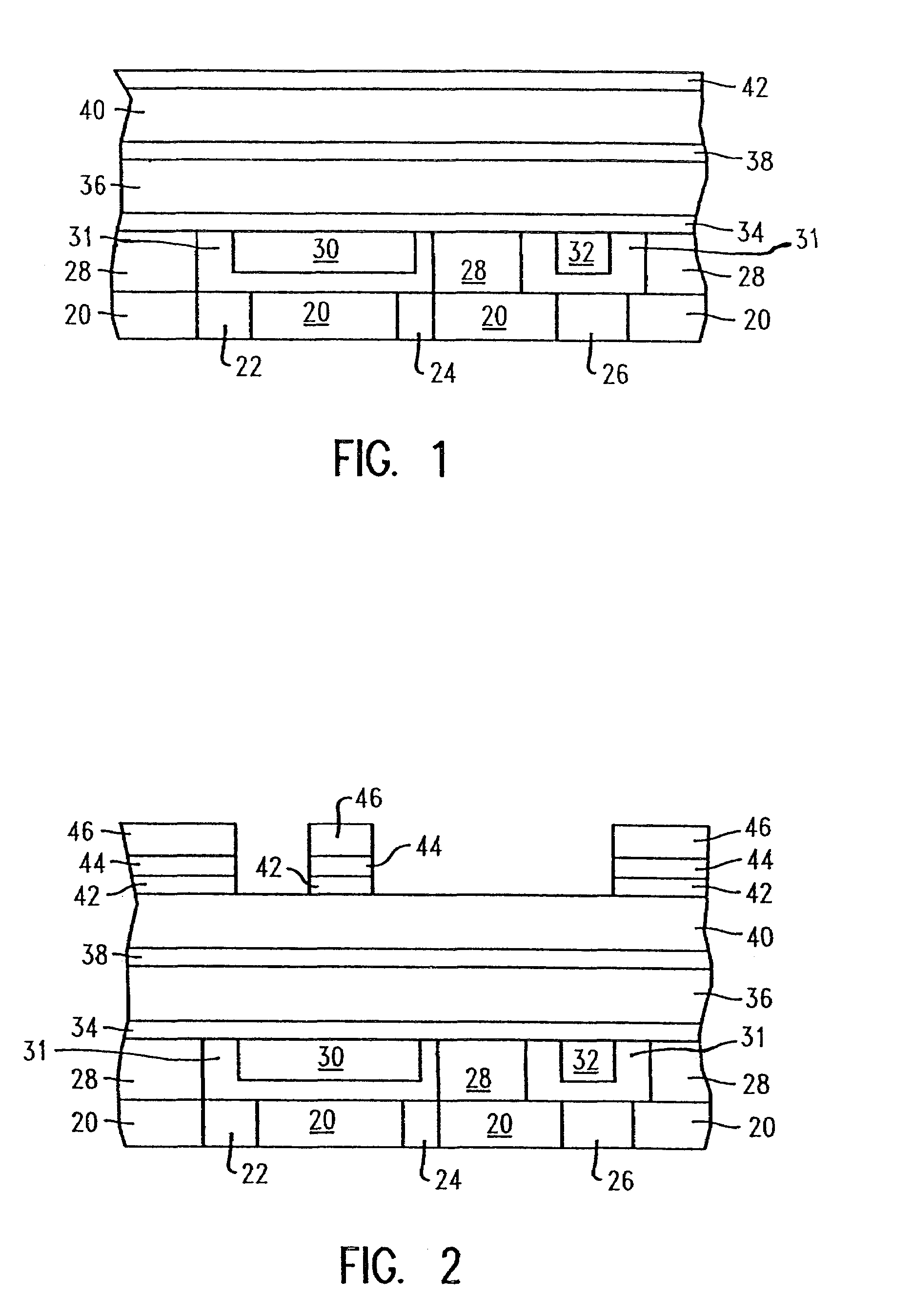
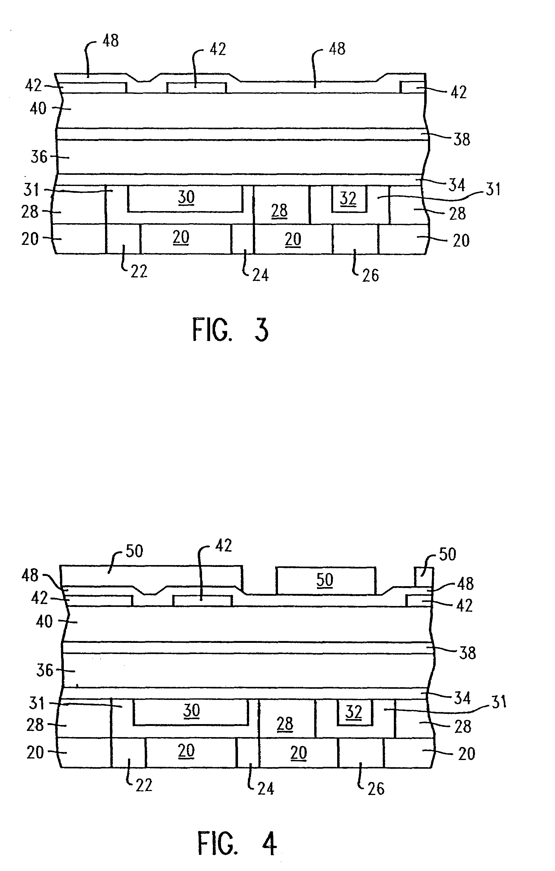
[0023]In describing the preferred embodiment of the present invention, reference will be made herein to FIGS. 1–12 of the drawings in which like numerals refer to like features of the invention. In a first embodiment, FIG. 1 depicts a dielectric stack deposited over a previously existing copper interconnect wiring level. The existing wiring level has a substrate dielectric layer 20 containing tungsten studs 22, 24, 26, over which is deposited dielectric layer 28 containing copper wires 30, 32 within TaN / Ta barrier layer 31. The dielectric layers may or may not be made of the same composition; for example, dielectric layer 20 may be phosphosilicate glass (PSG) while dielectric layer 28 may be undoped silicon glass (USG) or a glass containing silicon, carbon, oxygen and hydrogen (e.g., metholated SiOx, SiCOH). The dielectric stack consists of, in order from the bottom, a cap layer 34, e.g., silicon nitride Si3N4, an insulator layer with good mechanical properties and thermal conductiv...


PUM


Abstract

An adjustable self aligned low capacitance integrated circuit air gap structure comprises a first interconnect adjacent a second interconnect on an interconnect level, spacers formed along adjacent sides of the first and second interconnects, and an air gap formed between the first and second interconnects. The air gap extends above an upper surface of at least one of the first and second interconnects and below a lower surface of at least one of the first and second interconnects, and the distance between the spacers defines the width of the air gap. The air gap is self-aligned to the adjacent sides of the first and second interconnects.

Description

BACKGROUND OF INVENTION[0001]1. Field of the Invention[0002]The present invention relates to semiconductor devices and, in particular, to an adjustable, self-aligned air gap dielectric for low capacitance wiring in semiconductor devices.[0003]2. Description of Related Art[0004]Because of continuing decreases in size of circuit components in semiconductor chips, there are a number of interconnect wiring challenges facing the technical community over the next few technology generations. Among these challenges is the problem of undesirable capacitance in dielectric materials between circuit wiring. One avenue being pursued to lower interconnect capacitance is by the use of porous dielectrics. However, because these materials generally have reduced mechanical strength and thermal conductivity, it is more difficult to build the chip and dissipate heat during chip operation. Another challenge in the next few technology generations is presented by the expectation that the resistivity of co...

Claims


Application Information

Patent Timeline
Patent Type & Authority Patents(United States)
IPC IPC(8): H01L29/00H01L21/768H01L23/522H01L23/532
CPCH01L21/76811H01L21/7682H01L21/76831H01L23/5222H01L2924/0002H01L23/53295H01L2924/00H01L21/283H01L21/764H01L21/76H01L21/34
Inventor GEFFKEN, ROBERT M.MOTSIFF, WILLIAM T.
Owner GLOBALFOUNDRIES U S INC
Why Eureka
Try Eureka