

Electroluminescent devices
a technology of electroluminescent devices and electrodes, applied in the direction of luminescent compositions, organic semiconductor devices, chemistry apparatus and processes, etc., can solve the problems of difficult to inject holes into the emissive layer, difficult to find a preferable alternative, and many significant problems
- Summary
- Abstract
- Description
- Claims
- Application Information
AI Technical Summary
Benefits of technology
Problems solved by technology
Method used
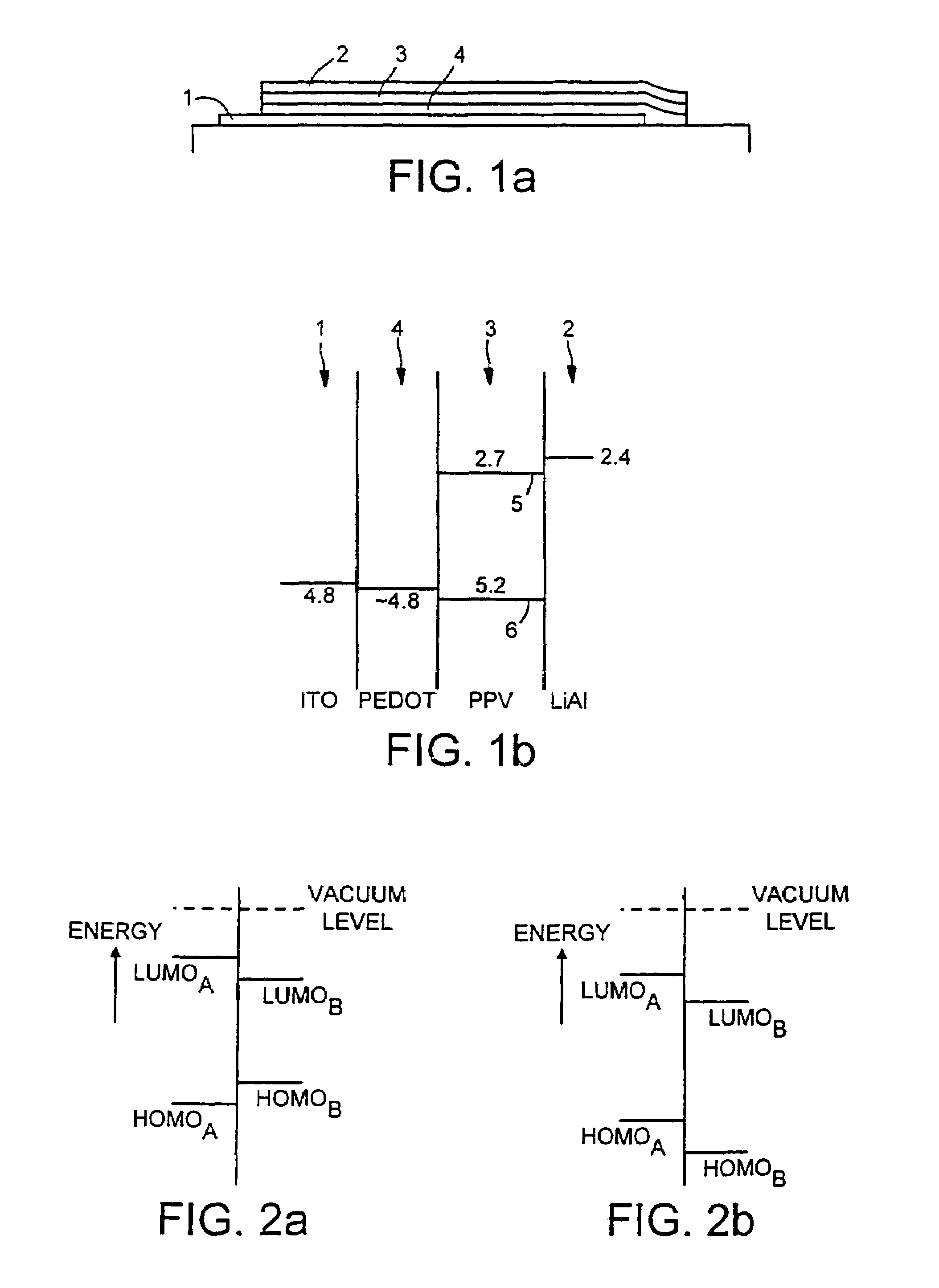
Image

Examples
Embodiment Construction
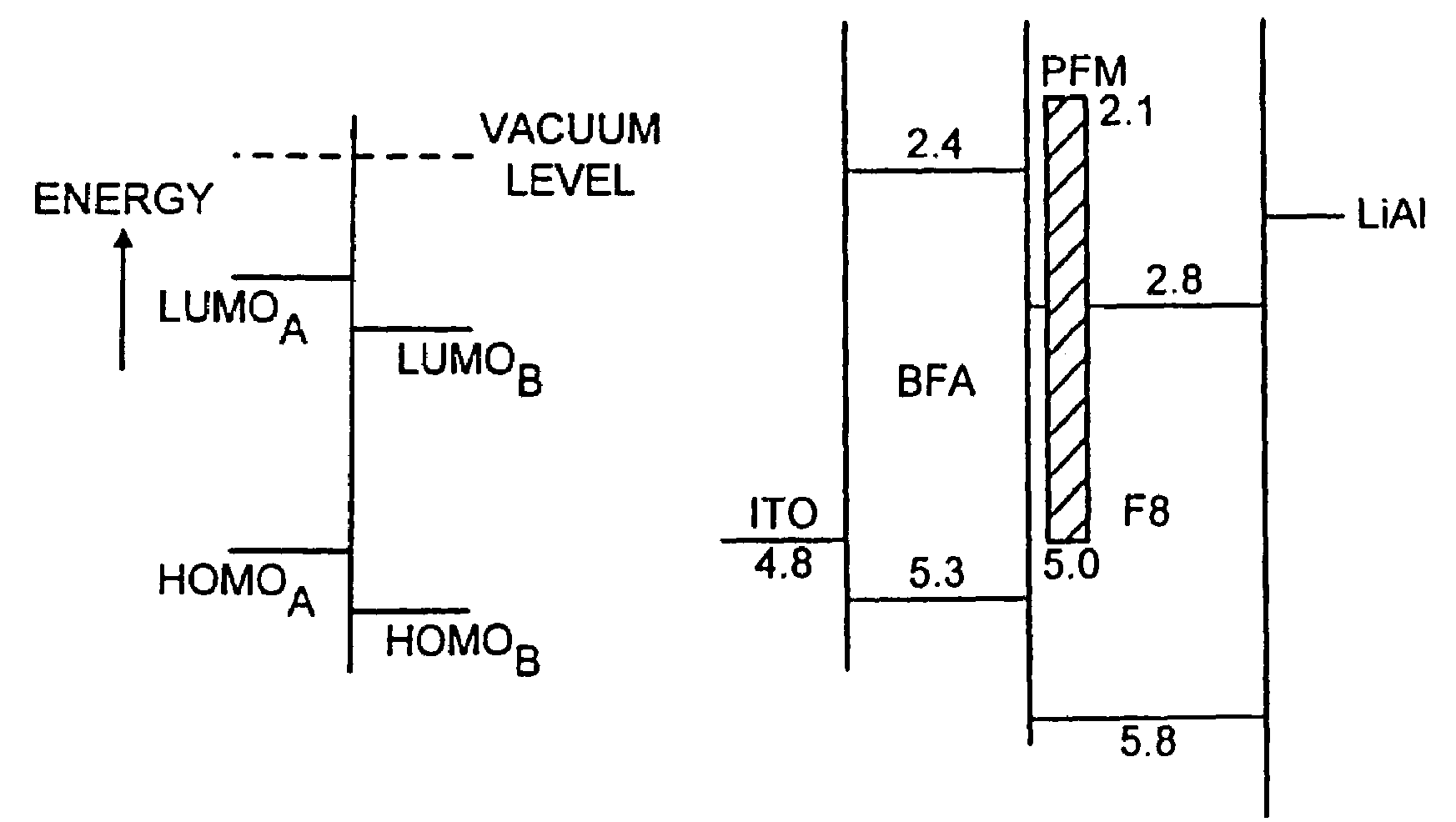
[0080]Table 1 gives material properties of some light-emissive materials:
[0081]
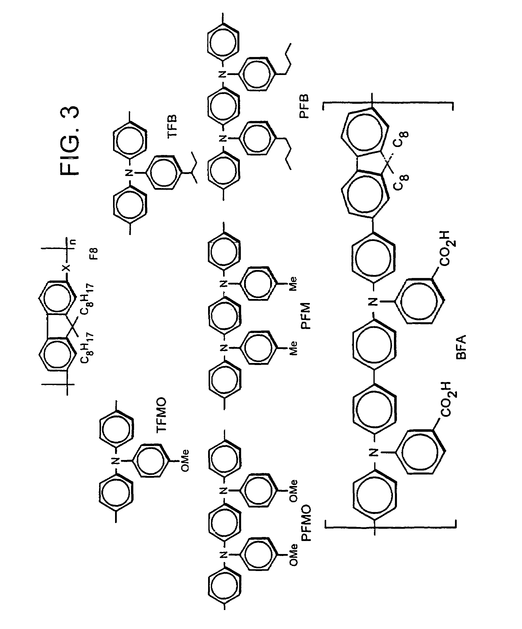
TABLE 1% PL% PLHOMOLUMOOpticalEmissionMaterialEfficiency1Efficiency2Level (eV)Level (eV)gap (eV)ColourF880505.82.83.0BlueTFB40155.32.33.0BluePFMO40135.02.03.0BluePFM2055.02.12.9Blue5F8BT95805.93.52.4GreenBis-DMOS5.73.52.2GreenPPVPPV A35.63.22.6GreenNotes to table 1:1Photoluminescence (PL) efficiencies measured using the technique of Halls et al. (see above).2Measured using a refined technique based on that of Halls et al.3See discussion of FIG. 25 below.
[0082]The HOMO positions were estimated from electrochemical measurement. The optical gaps were determined from the UV / visible absorbance spectrum. The LUMO positions were estimated from the HOMO position and the optical gap. 5F8BT is an abbreviation for a blend of 5% F8BT with 95% F8 w / w.
[0083]Of the blue emitters, F8 has the highest PL efficiency of these materials. Therefore, of these materials it would normally be the material of choice for a blue emis...
PUM
| Property | Measurement | Unit |
|---|---|---|
| HOMO energy level | aaaaa | aaaaa |
| HOMO energy level | aaaaa | aaaaa |
| HOMO energy level | aaaaa | aaaaa |
Abstract
Description
Claims
Application Information