Semiconductor device and method for fabricating the device

a technology of semiconductor devices and conductors, applied in semiconductor devices, semiconductor/solid-state device details, electrical apparatus, etc., can solve the problems of failure to directly bond through hole conductors to each other, and the reliability of electrical connection of through hole conductors is not guaranteed

Inactive Publication Date: 2006-07-18
RENESAS ELECTRONICS CORP +10
View PDF10 Cites 90 Cited by
  • Summary
  • Abstract
  • Description
  • Claims
  • Application Information

AI Technical Summary

Benefits of technology

[0005]Accordingly, the object of the present invention is to provide a semiconductor device and a method for fabricating the device capable of achieving reliable electrical connection by securely directly bonding conductors to each other even though their bonding surfaces are subjected to CMP and solid state bonding

Problems solved by technology

Therefore, when the first bonding surface and the second bonding surface are subjected to CMP, then dishing (a dish-shaped hollow) occurs on the surface of the through hole conductors, and this possibly leads to a fail in directly bonding the through hole conductors to each other.
That is, the electrical connection of the through hole conductors has no reliability.

Method used


Image

  • Semiconductor device and method for fabricating the device
  • Semiconductor device and method for fabricating the device
  • Semiconductor device and method for fabricating the device

Examples


first embodiment

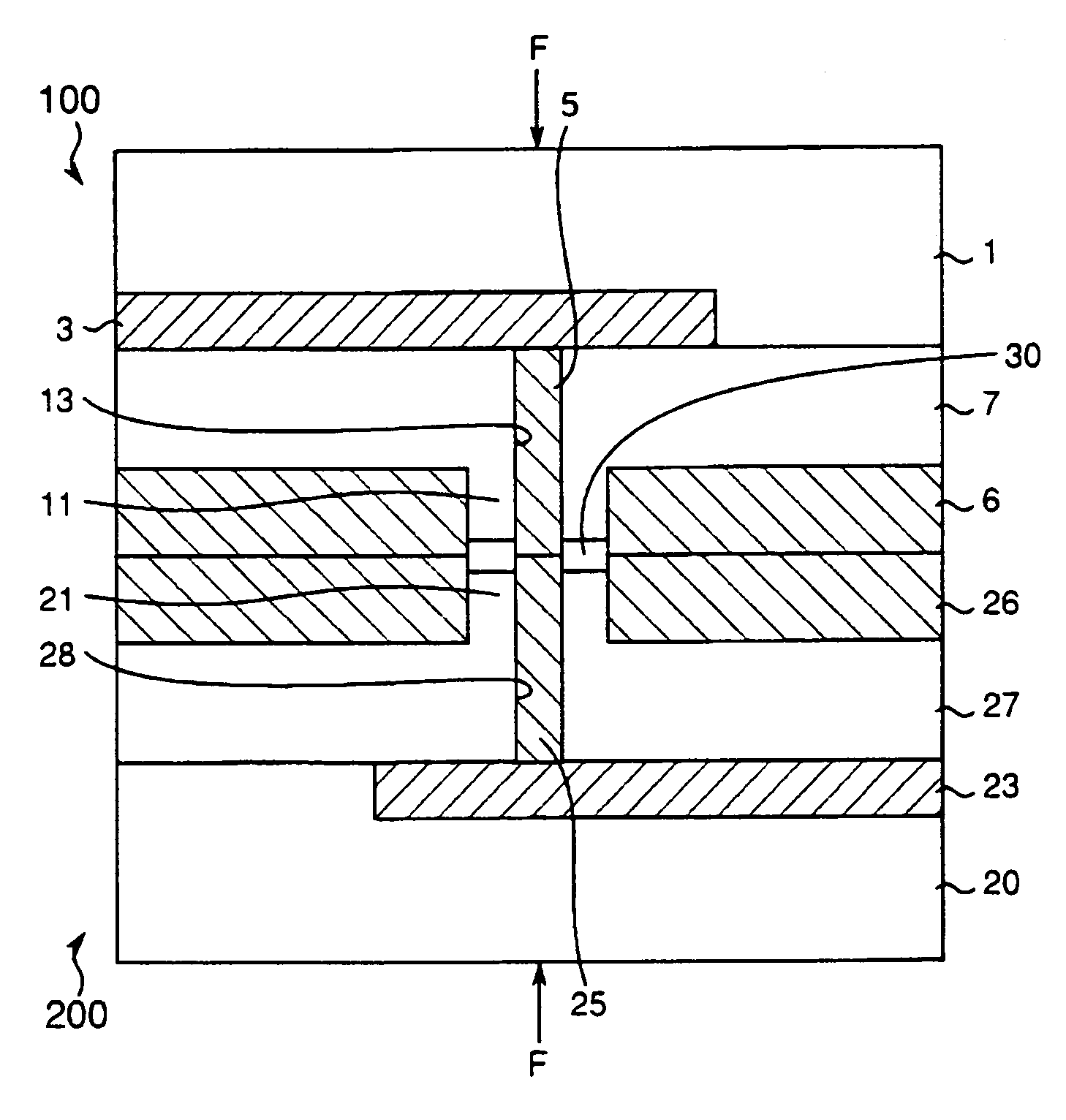
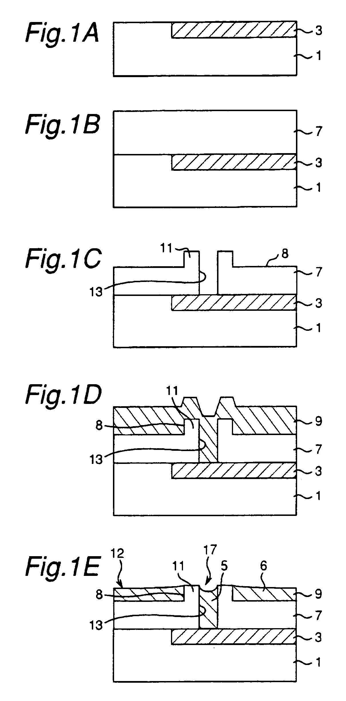
[0037]FIGS. 1A through 1E, 2A through 2C, 3 and 4 show a semiconductor device fabricating method of the First, as shown in FIG. 1A, a wiring layer 3 is provided as an example of a conductive layer on a semiconductor substrate ; that serves as an example of a first substrate. Further, as shown in FIG. 1B, an insulating layer 7 is laminated on the semiconductor substrate 1 and the wiring layer 3. The wiring layer 3 is made of a metal of, for example, copper, an aluminum alloy or the like, a polysilicon doped with an impurity, a silicide or the like, while the insulating layer 7 is made of, for example, silicon nitride.

[0038]Next, as shown in FIG. 1C, a through hole 13 that reaches the wiring layer 3 is formed through the insulating layer 7, and a grounding wiring groove 8 is formed on the insulating layer 7 by the techniques of photolithography and dry etching. A portion of the insulating layer 7 that is left between the through hole 13 and the grounding wiring groove 8 becomes a thr...

second embodiment

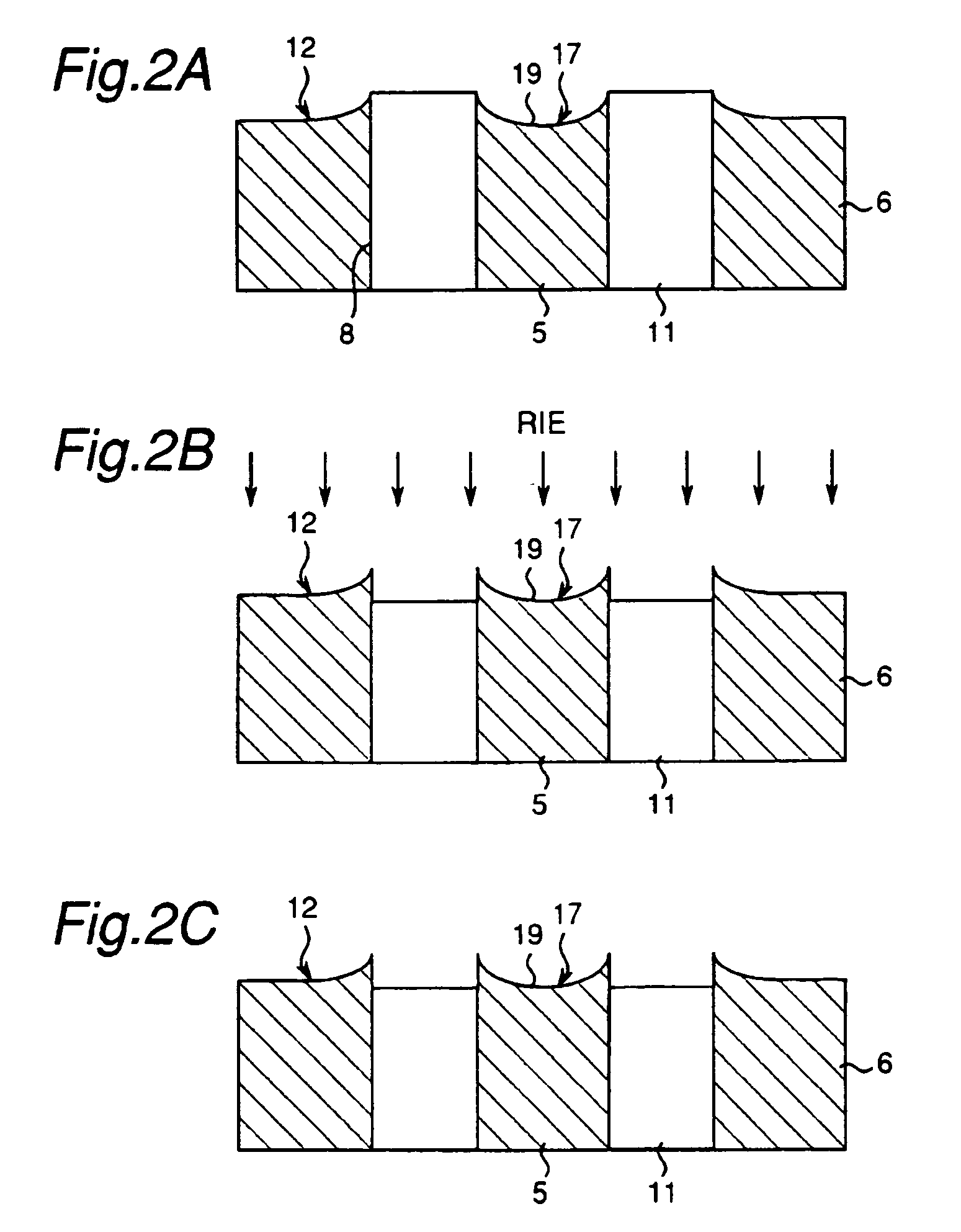
[0057]In the aforementioned first or second embodiment, the insulating regions (through hole insulators and insulating layer) 11, 21 and 37 surround the conductive regions (through hole conductors) 5, 25 and 35 on the bonding surfaces 12, 22 and 42. However, the insulating regions are not required to surround the respective conductive regions, and it is only required to provide the conductive regions and the insulating regions. It is also acceptable that one bonding surface has the conductive region and the insulating region while the other bonding surface has only the conductive region. According to the present invention, the insulating region is etched so that the dishing portion in the conductive region protrudes above the insulating region on the bonding surface polished by the CMP method. Therefore, the present invention can be applicable if at least one bonding surface has the conductive region and the insulating region.

[0058]According to the first or second embodiment, the th...


PUM


Abstract

There are provided a semiconductor device and method for fabricating the device capable of achieving reliable electrical connection by securely directly bonding conductors to each other even though bonding surfaces are polished by a CMP method and solid-state-bonded to each other. By polishing according to the CMP method, a through hole conductor 5 and a grounding wiring layer 10, which are made of copper, become concave in a dish-like shape and lowered in level, causing a dishing portion 17 since they have a hardness lower than that of a through hole insulator 11 made of silicon nitride. The through hole insulator 11 is selectively etched by a reactive ion etching method until the through hole insulator 11 comes to have a height equal to the height of a bottom portion 19 of the dishing portion 17 of the through hole conductor 5. The through hole conductors 5 and 25 are aligned with each other, and the bonding surfaces 12 and 22 are bonded to each other in a solid state bonding manner.

Description

BACKGROUND OF THE INVENTION[0001]The present invention relates to a semiconductor device that has a plurality of substrates and a method for fabricating the device.[0002]Lately, the present inventor has proposed this kind of semiconductor device obtained by laminating a conductive layer and an insulating layer on a first semiconductor substrate, polishing its surface by chemical mechanical polishing (hereinafter abbreviated to CMP) for the formation of a flat first bonding surface on which a silicon nitride film that serves as an insulating layer and copper that is a through hole conductor for plugging a through hole of the silicon nitride film are exposed, laminating a conductive layer and an insulating layer on a second semiconductor substrate, subjecting its surface to CMP for the formation of a flat second bonding surface on which a silicon nitride film and copper that is a through hole conductor are exposed, further applying pressure welding loads to the first semiconductor sub...

Claims


Application Information

Patent Timeline
Patent Type & Authority Patents(United States)
IPC IPC(8): H01L23/52H01L23/48H01L21/768H01L21/304H01L21/3205H01L23/498H01L23/522H01L25/065
CPCH01L23/49827H01L23/49833H01L23/5226H01L24/31H01L25/0657H01L2924/0002H01L2225/06513H01L2924/01004H01L2924/01013H01L2924/01029H01L2924/09701H01L2924/12044H01L2924/19041H01L2224/9202H01L2924/01005H01L2924/01006H01L2924/01033H01L2924/01068H01L2224/80895H01L2224/05572H01L2224/05552H01L2224/80894H01L2924/15787H01L2924/00H01L2924/00012H01L21/304
Inventor SUGA, TADATOMO
Owner RENESAS ELECTRONICS CORP
Why Eureka
Try Eureka