Silicon substrate apparatus and method of manufacturing the silicon substrate apparatus

a silicon substrate and silicon substrate technology, applied in the direction of electrical apparatus, modulation transference by distributed inductance and capacitance, semiconductor devices, etc., can solve the problems of inability to achieve satisfactory precision for forming waveguides, inability to pursue waveguide functions, and inability to achieve high-precision processing of waveguides

Inactive Publication Date: 2006-07-25
MITSUBISHI ELECTRIC CORP
View PDF16 Cites 6 Cited by
  • Summary
  • Abstract
  • Description
  • Claims
  • Application Information

AI Technical Summary

Problems solved by technology

If the waveguide is formed in the plastic member by the stamper method, satisfactory precision for forming the waveguide cannot be attained.
As a result, the waveguide cannot pursue a waveguide function.
If specifications of the frequency with which the waveguide is used are changed, the waveguide cannot be processed promptly with higher precision.
As a result, waveguides cannot be mass-produced.

Method used


Image

  • Silicon substrate apparatus and method of manufacturing the silicon substrate apparatus
  • Silicon substrate apparatus and method of manufacturing the silicon substrate apparatus
  • Silicon substrate apparatus and method of manufacturing the silicon substrate apparatus

Examples


Embodiment Construction

[0052]Embodiments according to the present invention will be described hereinafter with reference to the drawings.

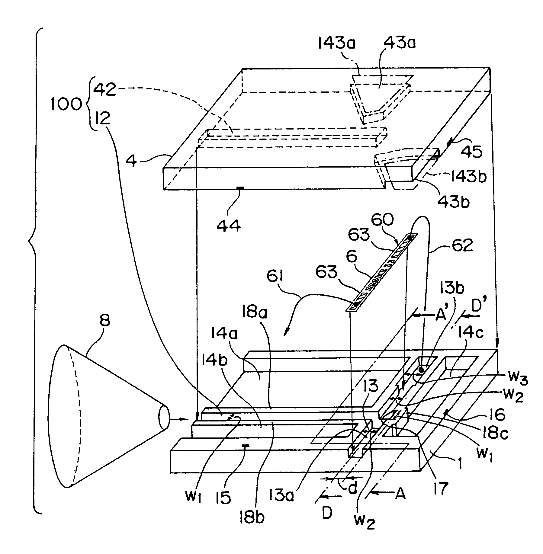
[0053]FIG. 1 is an exploded perspective view showing a structure of an SIS mixer device for use in a high frequency radio telescope according to one embodiment of the present invention. This SIS mixer device is disposed in a room cooled to a cryogenic temperature such as 4K or less, receives a radio wave of a frequency band such as 500 GHz band or the like, and converts a frequency of the radio wave. The SIS mixer device is characterized as follows. On an SIS device substrate 60, there are formed an SIS device 6 of a tunnel junction device having such a structure that an electronic insulator is put between a pair of superconductors, and conductor patterns 63 connected with the SIS device 6 to thereby constitute a filter circuit. The SIS device substrate 60 is put between a pair of silicon substrates 1 and 4 processed using a dry etching method related to the semiconducto...


PUM


Abstract

A first rectangular groove having a rectangular cross section and a second rectangular groove substantially orthogonal to the first rectangular groove and having a rectangular cross section are formed in a first silicon substrate. A third rectangular groove located at a position facing the first rectangular groove and having a rectangular cross section is formed on a second silicon substrate. A device substrate including a frequency conversion device is provided in the second rectangular groove, so that the frequency conversion device is located where the first and second rectangular grooves are orthogonal to each other. Further, the first silicon substrate on which the device substrate is located is bonded to the second silicon substrate, so that the first rectangular groove opposes the third rectangular groove, forming a rectangular waveguide which includes the first rectangular groove and the third rectangular groove, and in which a received high frequency signal propagates and is incident on the frequency conversion device.

Description

TECHNICAL FIELD[0001]The present invention relates to a silicon substrate apparatus having a rectangular waveguide formed therein, which is used in a high frequency receiver, and also, to a method of manufacturing a silicon substrate apparatus.Background Art[0002]In a millimeter waveband or sub-millimeter waveband radio telescope, a heterodyne receiver that employs a waveguide mixer has been conventionally used. An SIS device substrate, having an SIS (Superconductor-Insulator-Superconductor) device including a tunnel junction, having a structure with an electric insulator between a pair of superconductors and conductor patterns connected with the SIS device and constituting a filter circuit , is cooled to 4K and used as a mixer device circuit. As shown in, for example, Japanese patent laid-open publication No. 6-216653 (hereinafter, referred to as the first prior art), an aluminum block is processed by machining, to form a waveguide in which a high frequency received signal and a lo...

Claims


Application Information

Patent Timeline
Patent Type & Authority Patents(United States)
IPC IPC(8): H01L21/00H03D9/06
CPCH03D9/0616
Inventor KUMAGAI, MUNEHITOYOSHIDA, YUKIHISAMATSUURA, TSUKASAHONMA, YUKIHIRO
Owner MITSUBISHI ELECTRIC CORP
Why Eureka
Try Eureka