Scanning probe microscopy probes and methods

a microscopy and scanning probe technology, applied in the field of scanning probe microscopy, can solve the problems of existing fabrication methods, sharp tips, and performance limiting devices of the scanning probe's cantilever beam with integrated tips

Inactive Publication Date: 2006-07-25
THE BOARD OF TRUSTEES OF THE UNIV OF ILLINOIS
View PDF9 Cites 39 Cited by
  • Summary
  • Abstract
  • Description
  • Claims
  • Application Information

AI Technical Summary

Problems solved by technology

Needless to say, the SPM probe's cantilever beam with integrated tip is a performance limiting device in the overall scanning probe microscope system.
There are a number of major drawbacks to existing fabrication methods.
First, the tips are made sharp using a special, time-sensitive processes that is not very efficient.
Additionally, it is difficult to produce large arrays of tips with uniform sharpness.
However, microcontact printing invariably requires a dedicated photolithography mask to produce inverse mold features, and is limited with respect to multi-ink and alignment registration capabilities.
Additionally, the production of the mask can be relatively costly and time consuming, particularly when sub-micrometer features are desired.

Method used


Image

  • Scanning probe microscopy probes and methods
  • Scanning probe microscopy probes and methods
  • Scanning probe microscopy probes and methods

Examples


example

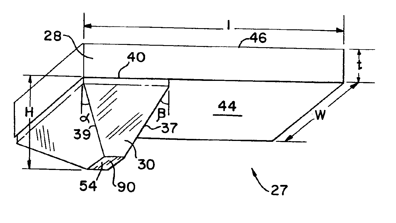
[0058]The probe 227 was mounted and tested on a Thermomicroscopes AutoProbe® M5 atomic force microscope (AFM). An organic molecule, 1-octadecanethiol (ODT), was used for the fluid 60. ODT (98%) may be obtained from Aldrich Chemical Company (Milwaukee, Wis.). The substrate 62 was a silicon chip coated with a 5-nm-thick chrome layer for adhesion promotion, and a 30-nm-thick gold layers. Preferably, the substrate 62 is formed from a single crystal silicon wafers ({100} orientation), which may be obtained from International Wafer Service (Portola Valley, Calif.). Gold (99.99%) for the gold layers may be obtained from Pure Tech (Brewster, N.Y.). A chromium evaporation source (chrome plated tungsten rod) to form the chrome layer may be obtained from R. D. Mathis Company (Long Beach, Calif.). A contact inking method, as described in “Contact-Inking Stamps for Microcontact Printing of Alkanethiols on Gold”, by L. Libioulle, A. Bietsch, H. Schmid, B. Michel, and E Delamarche, Langmuir, 1999,...


PUM

PropertyMeasurementUnit
heightaaaaaaaaaa
heightaaaaaaaaaa
lengthaaaaaaaaaa

Abstract

A method for fabricating scanning probe microscopy (SPM) probes is disclosed. The probes are fabricated by forming a structural layer on a substrate, wherein the substrate forms a cavity. A sacrificial layer is located between the substrate and the structural layer. Upon forming the structural layer, the sacrificial layer is selectively removed, and the probe is then released from the substrate. The substrate may then later be reused to form additional probes. Additionally, a contact printing method using a scanning probe microscopy probe is also disclosed.

Description

RELATED APPLICATION DATA[0001]The present application is a divisional of U.S. application Ser. No. 10 / 440,022, filed May 16, 2003, which is incorporated herein by reference to the extent permitted by law.FEDERALLY SPONSORED RESEARCH OR DEVELOPMENT[0002]This invention was made with Government support under the National Science Foundation under the NSF Program (Grant No. 0118025), DARPA Grant No. DAAD-19-00-1-0414 and AFOSR Grant No. F49620-00-1-0283. The government may have certain rights in this invention.BACKGROUND[0003]This invention relates generally to scanning probe microscopy (hereinafter “SPM”), and in particular, to an SPM probe formed with an integrated tip and to a method of printing with an SPM probe.[0004]A scanning probe microscope is an important instrument for science and technology. One of the first scanning probe microscopes ever developed was called a Scanning Tunneling Microscope (STM). Another device within the scanning probe microscope family is an Atomic Force ...

Claims


Application Information

Patent Timeline
Patent Type & Authority Patents(United States)
IPC IPC(8): G01N23/00B05D5/00B29C33/76B29C59/00B81B1/00B81B3/00B82B3/00G01Q60/00G01Q70/16G01Q80/00G03F7/00
CPCB82Y10/00B82Y35/00B82Y40/00G01Q70/06G03F7/0002G01Q70/16B82Y30/00Y10S977/877G01Q80/00Y10S977/86Y10S977/875Y10S977/857
Inventor LIU, CHANGZOU, JUNWANG, XUEFENGBULLEN, DAVID
Owner THE BOARD OF TRUSTEES OF THE UNIV OF ILLINOIS
Why Eureka
Try Eureka