Solid-state image pickup device and manufacturing method for the same

a solid-state image and pickup device technology, applied in the direction of color television, television system, radio control device, etc., can solve the problems of reducing the size of pixels, increasing the reading voltage and reducing the height difference between electrodes and others to a greater degree than currently achieved, so as to reduce the height difference of the substrate surface, reduce the reading voltage, and prevent the effect of smear characteristics from being reduced

Active Publication Date: 2006-08-01
SONY SEMICON SOLUTIONS CORP
View PDF1 Cites 28 Cited by
  • Summary
  • Abstract
  • Description
  • Claims
  • Application Information

AI Technical Summary

Benefits of technology

[0013]Therefore, an object of the present invention is to reduce the reading voltage through prevention of the smear characteristics from being reduced in association with size reduction of the unit pixel, through reduction of height difference of the substrate surface, and through influence suppression of the accumulation layer over the photoelectric conversion regions.

Problems solved by technology

As a result, the potential at the position shows less change with respect to the reading voltage, problematically increasing the reading voltage to a greater degree.
With the concern for maintaining the pixel properties, however, it has been difficult to reduce the height difference of electrodes and others to a greater degree than currently achieved.
Thus, reducing the pixels in size may reduce the light-gathering capability.
The issue here is that such a structure has the following problems as forming a groove on the surface of a substrate for use as a channel opposing to a charge reading electrode and a charge transfer electrode.
Thus, reducing the height difference of the polysilicon electrode is difficult.
As a result, the potential at the position shows less change with respect to the reading voltage, failing to solve the problem of increasing reading voltage.
Here, even when a light-shielding film is formed to cover the polysilicon electrode may be a possibility, the resulting film simply covers the polysilicon electrode on the surface of the substrate, failing to fully achieve the expected light-shielding effect, and reducing the smear characteristics.
Moreover, although reducing the reading section in width may be an effective option for voltage reduction, this easily causes blooming.

Method used


Image

  • Solid-state image pickup device and manufacturing method for the same
  • Solid-state image pickup device and manufacturing method for the same
  • Solid-state image pickup device and manufacturing method for the same

Examples


first embodiment

(First Embodiment)

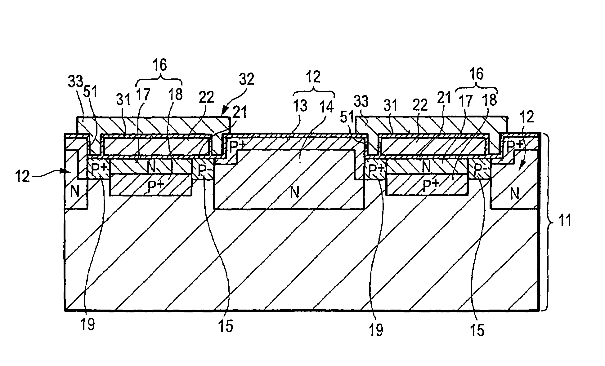
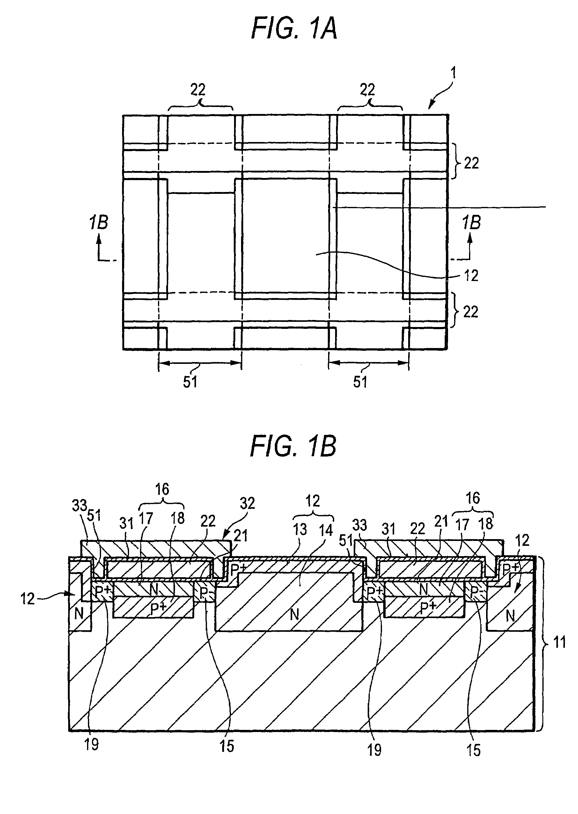
[0035]By referring to FIGS. 1A and 1B, a solid-state image pickup device of a first embodiment is described. Specifically, FIG. 1A is a plan view of layout, and FIG. 1B is the schematic cross-sectional view cut along a line 1B—1B of FIG. 1A.

[0036]As shown in FIGS. 1A and 1B, in a solid-state image pickup device 1, a substrate 11 is formed with a groove 51. The groove 51 is formed in a region to which an electrode is formed in a transfer register direction (vertical transfer direction), for example. The groove 51 has the depth of 0.01 μm to 5 μm from the surface of the substrate 11, for example. This depth is about the same or less as that of a bonding section between a hole accumulation layer 13 and an N-type layer 14, both of which are formed on a photoelectric conversion region 12. The substrate 11 is a semiconductor substrate, e.g., silicon substrate. The groove 51 and the photoelectric conversion region 12 are formed adjacent to each other. The photoelectric co...

second embodiment

(Second Embodiment)

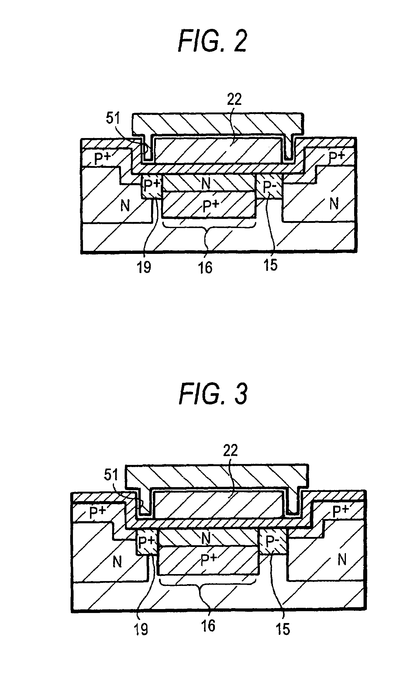
[0040]Described next is a solid-state image pickup device of a second embodiment of the present invention by referring to the schematic cross-sectional view of FIG. 2.

[0041]As shown in FIG. 2, the structure of the second embodiment is the same as that of the first embodiment except the following. That is, as to the electrode 22, its parts in the transfer register direction (vertical transfer direction) are formed, in the groove 51, at least partially on the pixel separation region 19, and on the vertical register 16 and the reading gate 15.

third embodiment

(Third Embodiment)

[0042]Described next is a solid-state image pickup device of a third embodiment of the present invention by referring to the schematic cross-sectional view of FIG. 3.

[0043]As shown in FIG. 3, the structure of the third embodiment is the same as that of the first embodiment except the following. That is, as to the electrode 22, parts in the transfer register direction (vertical transfer direction) are formed, in the groove 51, at least partially on the pixel separation region 19, and partially on the vertical register 16, and the reading gate 15.

[0044]With the electrode 22 formed as such in the second and third embodiments, the same effects as described in the first embodiment can be achieved, e.g., reduction of the smear characteristics, and reduction of the reading voltage. At the time of manufacturing the electrode 22 and others, any displacement caused by mask alignment in a lithography process becomes favorably allowable. As such, from a manufacturing viewpoint...


PUM


Abstract

A solid-state image pickup device includes, in a substrate, a plurality of photoelectric conversion regions for subjecting incoming light to photoelectric conversion, a reading gate for reading a signal charge from the photoelectric conversion regions, and a transfer register (vertical register) for transferring the signal charge read by the reading gate. Therein, a groove is formed on the surface side of the substrate, and the transfer register and the reading gate are formed at the bottom part of the groove. With such a structure, in the solid-state image pickup device, reduction can be achieved for the smear characteristics, a reading voltage, noise, and others.

Description

[0001]The present application claims priority to Japanese Patent Application JP2003-098783, filed in the Japanese Patent Office Apr. 2, 2003; and Japanese Priority Document JP2003-390305, filed in the Japanese Patent Office Nov. 20, 2003, the entire contents of which are incorporated herein by reference.BACKGROUND OF THE INVENTION[0002]1. Field of the Invention[0003]The present invention relates to a solid-state image pickup device and a manufacturing method therefor and, more specifically, to a solid-state image pickup device operating in an interlace mode with a light shielding film provided, and a manufacturing method therefor.[0004]2. Description of the Related Art[0005]A solid-state image pickup device of a conventional type operating in an interlace mode is structured by a flat N-type silicon substrate 111 formed thereon with a photoelectric conversion region 112 as shown in FIGS. 16A and 16B. Specifically, FIG. 16A is the layout view, and FIG. 16B shows the schematic cross-se...

Claims


Application Information

Patent Timeline
Patent Type & Authority Patents(United States)
IPC IPC(8): H01L31/062H01L27/148H01L27/14H01L27/146H01L31/10H04N5/335H04N5/359H04N5/369
CPCH01L27/14843H01L27/14837H01L27/14689H01L27/14623H01L27/148H01L31/10
Inventor KITANO, YOSHIAKIKARASAWA, NOBUHIROKUROIWA, JUNABE, HIDESHISATO, MITSURUOHKI, HIROAKI
Owner SONY SEMICON SOLUTIONS CORP
Why Eureka
Try Eureka